
IEDM 2017 + ISSCC 2018: Intel’s 10nm, switching to cobalt interconnects
![]() At the 2017 IEEE International Electron Devices Meeting (IEDM) in San Francisco, Intel formally detailed its 10-nanometer process technology. This leading-edge process is expected to be utilized by many of their future products, including their FPGAs and desktop and server microprocessors.
At the 2017 IEEE International Electron Devices Meeting (IEDM) in San Francisco, Intel formally detailed its 10-nanometer process technology. This leading-edge process is expected to be utilized by many of their future products, including their FPGAs and desktop and server microprocessors.
The 10 nm process was presented by Chris Auth, vice president at Intel Corporation and the director of advanced transistor development. Auth was responsible for leading the development of Intel’s 10 nanometer high-performance CMOS logic transistor process.
![]() Because this article was planned for late January, we’ve decided to withhold publication and incorporate additional 10nm details from the 65th International Solid-State Circuits Conference (ISSCC) which was held earlier this week. At ISSCC, Zheng Guo presented Intel’s 10nm SRAM devices which are discussed later in this article.
Because this article was planned for late January, we’ve decided to withhold publication and incorporate additional 10nm details from the 65th International Solid-State Circuits Conference (ISSCC) which was held earlier this week. At ISSCC, Zheng Guo presented Intel’s 10nm SRAM devices which are discussed later in this article.
Overview
The major features are:
- 2.7x density over their 14nm
- 3rd generation FinFET transistors
- Self-Aligned Quad-Patterning (SAQP)
- Contact-over-active-gate (COAG)
- Cobalt local interconnect, vias, and trench contacts
- Cobalt interconnect liners
Design Features
Intel’s 10 nanometer largely builds on many of their existing technologies.
- 2nd generation Low-κ spacer
- 3rd generation of fully depleted FinFET transistors
- 5th generation High-κ metal gate
- 7th generation strain silicon
- Self-Aligned Quad Patterning (SAQP) for the critical patterning layers (3 critical layers)
- 4 workfunction metals on the base process
- Self-Aligned trench contact
They first introduced their fully-depleted FinFET structures at the 22 nm node and most recently in their 14 nm node. Likewise, the High-κ gate was first introduced in their 45 nm node and have been used ever since. It’s worth pointing out that in addition to the 4 workfunction metals used for the base process, Intel noted that they also have 6 workfunction metals that can be introduced for high-Vth transistors when needed.
Beyond Conventional Scaling
While the time between each consecutive technology nodes have lengthened, Intel has attempted to compensate for this by accelerating the density of each process. Going from the 22-nanometer node down to the 14-nanometer, transistor density increased by 2.5x. Likewise, going from the 14-nanometer down to the 10-nanometer node we see a 2.7x increase in density. In other words, from the introduction of the 22 nm node in late 2011 to the ramp-up of Intel’s 10 nm in 2018 we have observed close to 7x density increase over the span of 7 years.
Key Dimensions
The key transistor dimensions for Intel’s 10nm are:
| Intel 10nm Process | ||
|---|---|---|
| Feature | Pitch | Scaling |
| Fin | 34 nm | 0.81x |
| Gate | 54 nm | 0.77x |
| M0 | 40 nm | 0.71x |
| M1 | 36 nm | 0.51x |
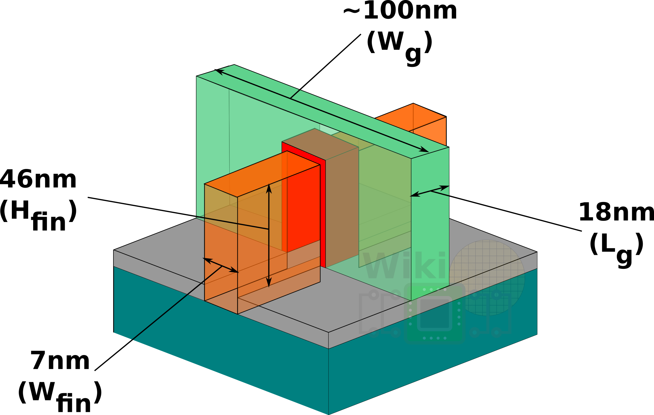
For their 10nm paper, Intel used a 46 nm fin height transistor (although that’s discussed further later on) with a pitch of 7nm and a gate length of 18nm. This roughly translate to around 100nm gate width. Below is a rough diagram of the features:
In order to enable a pitch down to 34 nanometers, such as in the case of the fin pitch and the minimum metal layer, Intel has moved to self-aligned quadruple patterning (SAQP). Dual patterning (SADP) was first introduced at the 22nm node and is continued to be used for the down to the 44nm pitch. For the wider pitch, single patterning is used.
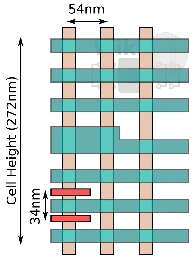
At 272nm cell height and 34nm fin pitch, there are eight lines that can be used. It’s worth noting that Intel uses different cells for different applications.
–
Spotted an error? Help us fix it! Simply select the problematic text and press Ctrl+Enter to notify us.
–