
IEDM 2017 + ISSCC 2018: Intel’s 10nm, switching to cobalt interconnects
Hyperscaling
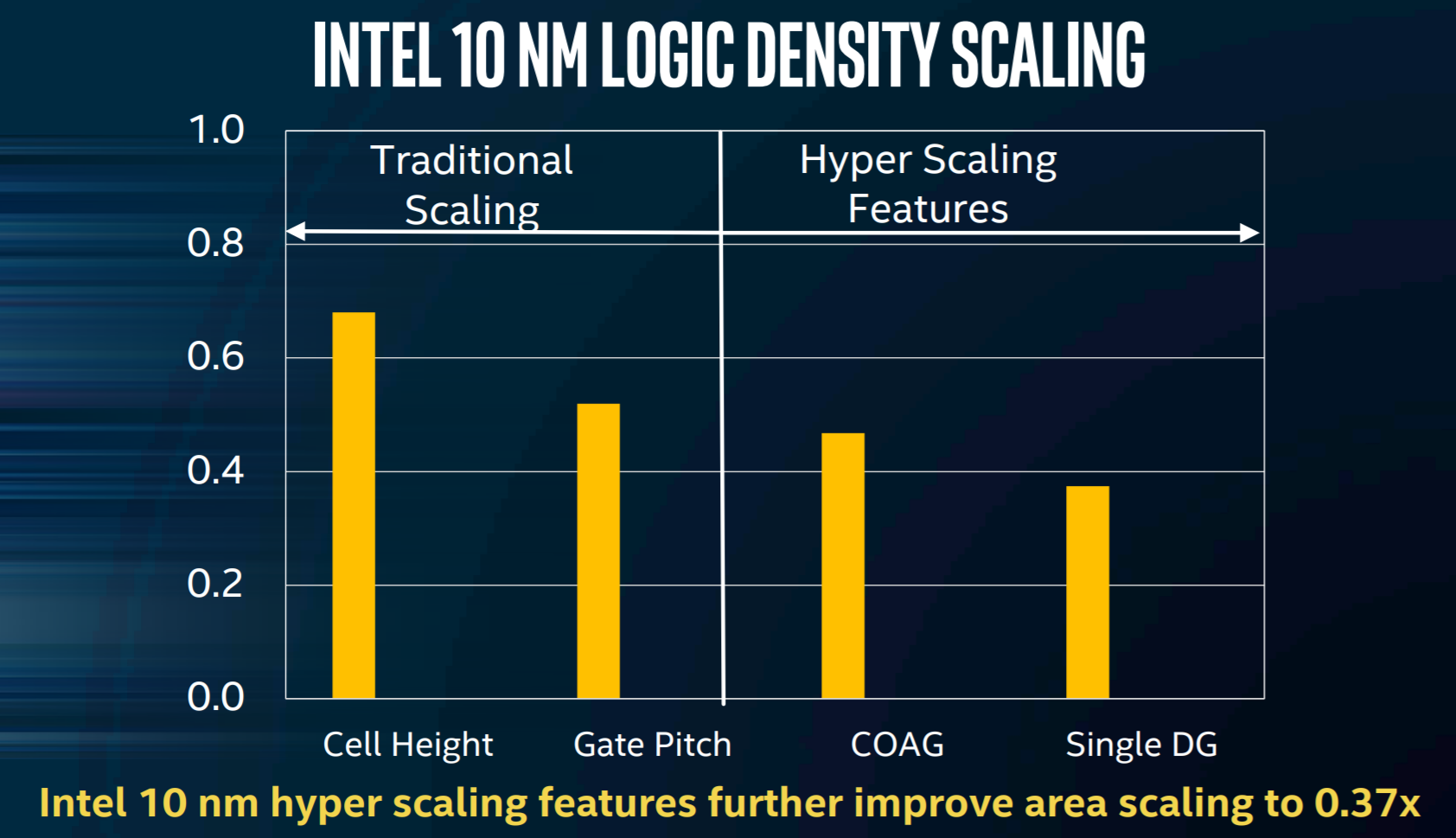
Intel has introduced a new marketing term along with their 10nm process – “Hyperscaling”. Despite some claims to the contrary, there is very real technology behind it. In addition to using self-aligned quad-patterning (SAQP) for the critical layers, Intel introduced two novel transistor-related accelerators in order to extract higher density: Intel addressed the isolation at the cell boundary and introduced a new feature called contact over active gate (COAG).
Single Dummy Gate
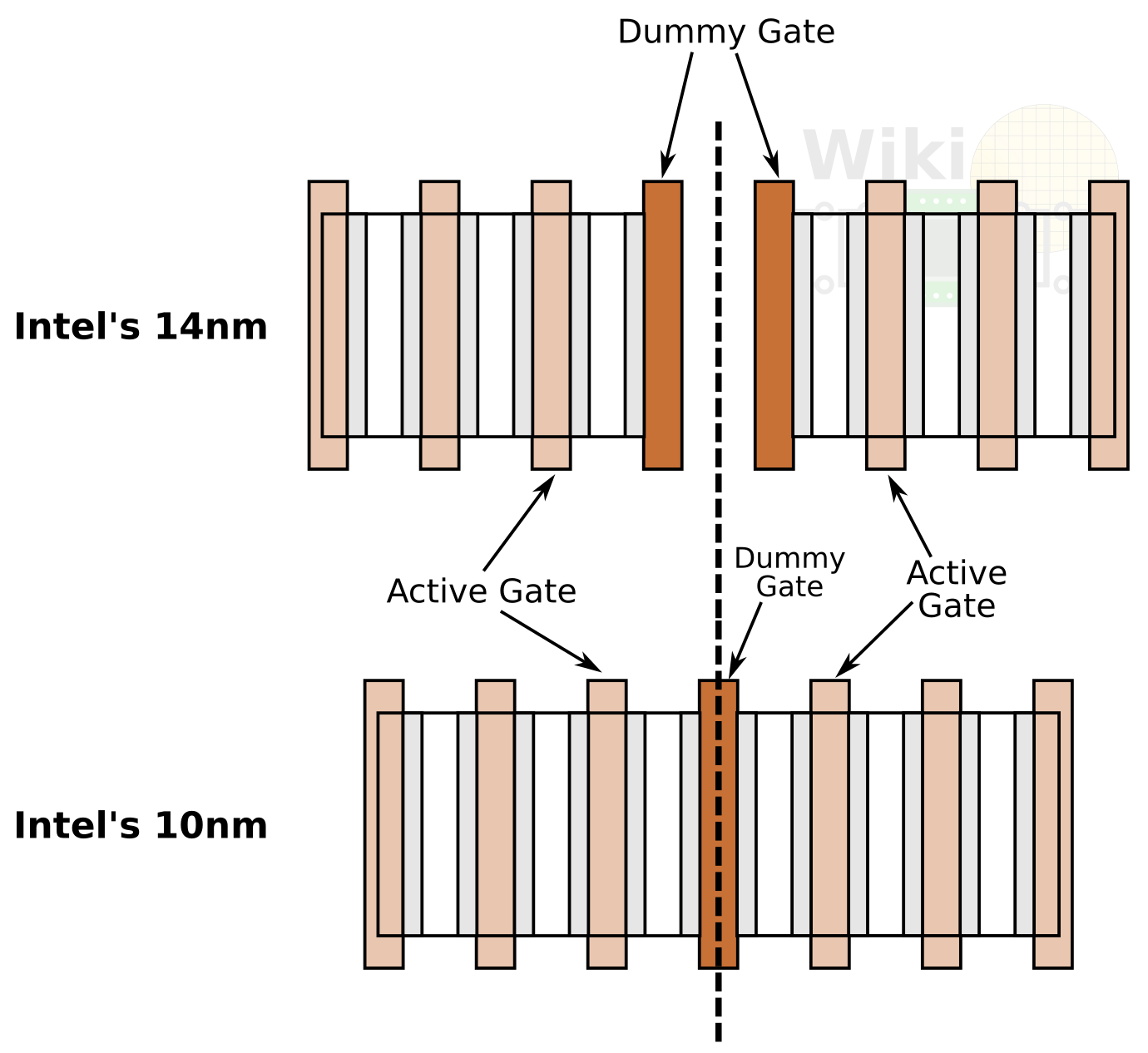
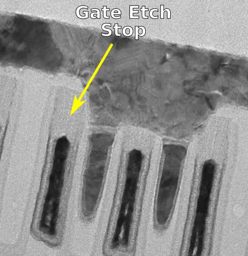
The first thing Intel addressed is the isolation at the cell boundary. Traditionally, at your cell boundary you have the last active gate, the active diffusion and then a dummy gate right across the cell boundary. For their 14nm process, this meant that there was a dummy gate at the edge of each cell.
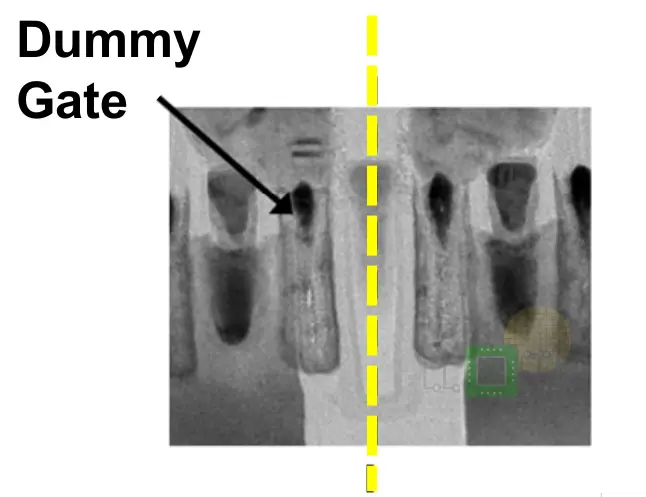
At the 10nm process Intel has merged the cell boundaries across cells into a single dummy gate – i.e. there is now a single dummy gate spacing between the end active fins which means they have effectively eliminated one poly track. Intel claims this provides around 20% area saving.
It’s worth pointing out that despite its name, in practice there’s just the etched line spacing and not an actual dummy gate. The TEM below from ISSCC 2018 shows it clearly.
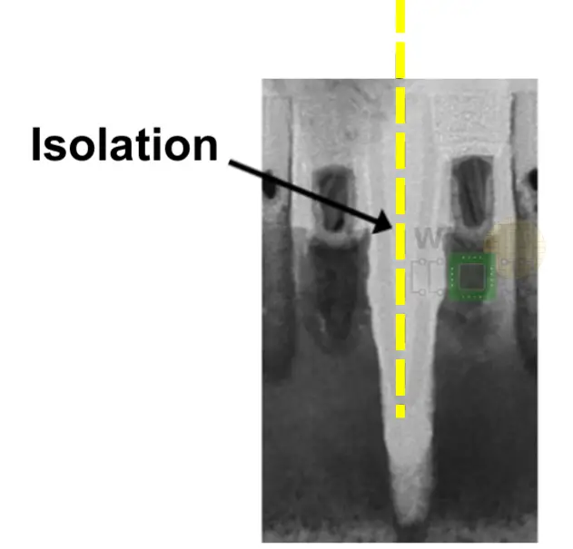
Interestingly, the etch goes really far down, very similar to what TechInsights found Samsung has done with their 10nm process, in order to separate the cells.
Contact Over Active Gate (COAG)
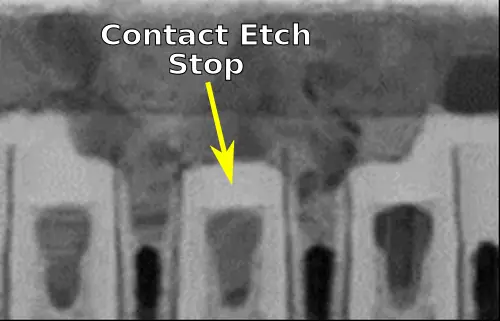
The second feature Intel has introduced is the contact over active gate (COAG). Traditionally, as shown below with the single transistor, you extend the gate over the isolation and then drop the gate via over the gate. What Intel has done with their 10nm process is allow the gate via to be dropped directly over the active area which allows for further reduction of the cell height. Intel reported a cell reduction of 10% by using COAG.
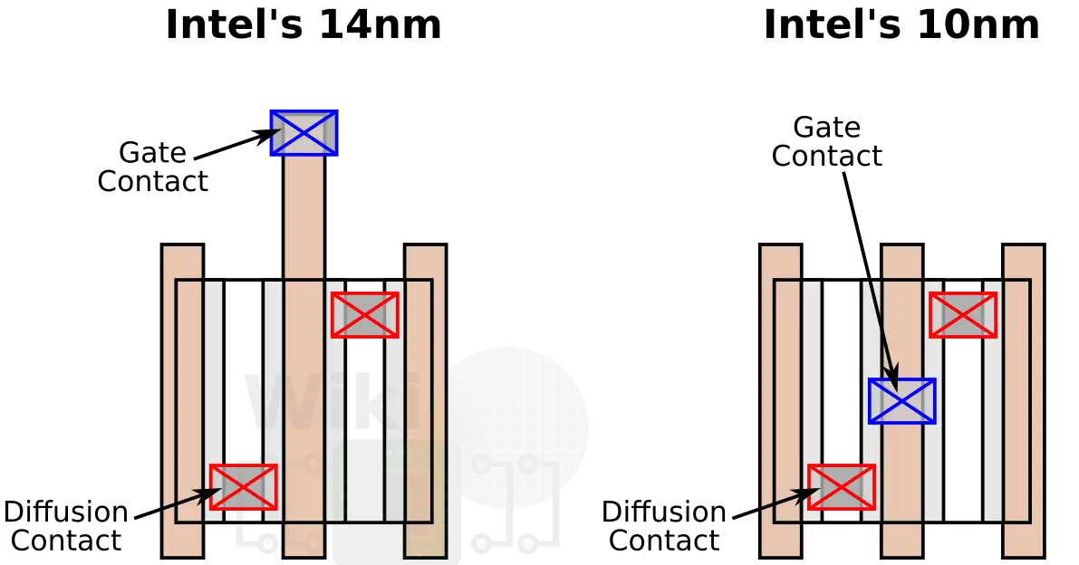
This is a pretty complex change which involves using a self-aligned contacts process for the diffusion contact and gate contact. Intel has been using self-aligned diffusion contacts since their 22nm node to form tight contact to gate overlays so this is another flow extension. This is done by recess filling and polishing the gate back to leave the silicon nitride etch-stop material in the cavity to prevent the diffusion contact from shorting the gate.
For this 10nm technology, they extended the flow with an additional recess of the diffusion contact and the deposition of a silicon carbide etch-stop layer to prevent the gate contact from shorting the diffusion contact. Since the underlying material remains unharmed, both the diffusion and gate vias shows excellent selectivity. Overall, this adds three additional steps – one etch, one dep, and one polish, but it allows the gate contacts to land on the active area itself.
More Aggressive Scaling
In total, with the help of extra optimizations techniques such as COAG, Intel achieved a better-than-normal scaling of 0.37x.
–
Spotted an error? Help us fix it! Simply select the problematic text and press Ctrl+Enter to notify us.
–