
IEDM 2017 + ISSCC 2018: Intel’s 10nm, switching to cobalt interconnects
Back-End
Intel 10nm process consists of a 13-layer metallization stack.
| Intel 10nm Metallization Stack | ||
|---|---|---|
| Layer | Pitch | TEM |
| M0 | 40 nm | TEM of the metal stack. Note that the upper-most layer is the TM0 (TM1 and bumps are not shown).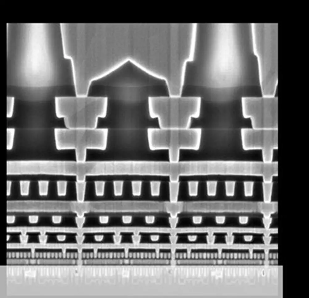 (Intel, IEDM 2017) |
| M1 | 36 nm | |
| M2 | 44 nm | |
| M3 | 44 nm | |
| M4 | 44 nm | |
| M5 | 52 nm | |
| M6 | 84 nm | |
| M7 | 112 nm | |
| M8 | 112 nm | |
| M9 | 160 nm | |
| M10 | 160 nm | |
| TM0 | 1,080 nm | |
| TM1 | 11 μm | |
For the critical dimensions which is 34 nm fins and the two metal layers, Intel uses quad patterning which adds four steps to the flow – deposition on the spacers followed by the etching steps. Metals 2 through 5 as well as the gate patterning get away with just double patterning.
Going Cobalt
As you shrink the transistor geometry you need to shrink the wires as well for the chip to benefit from the higher density. Scaling the wires has been an increasingly complicated task. While the solutions are incredibly complex, the fundamental problem is simple – the longer and narrower the wires get, the higher the electrical resistance is.
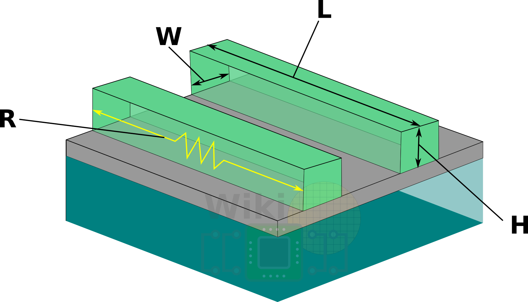
Using the incredibly over-simplified interconnect structure above for RC analysis, the resistance of the wire can be described as R = Ï â‹… [L / (W â‹… H)] where Ï is electrical resistivity of the interconnect, L is the length of the wire, and (W * H) is the cross-sectional area.
Exactly 20 years ago, at IEDM 1997, Daniel Edelstein, an IBM Fellow, presented their paper announcing their plan to insert a Cu BEOL technology into production. IBM ramped up their 180nm process (CMOS-8S3) in 1998 which was later used for the POWER4 chips. At the 180nm process IBM replaced the Aluminum interconnect with copper for its significantly lower resistivity, higher scalability, and higher current density capabilities.
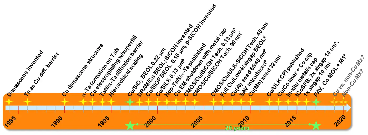
Included are several achieved first by other companies (*), and two which were suspended (#).
(Source: IBM, IEDM 2017)
20 years and 10 technology nodes later, we’re finally see copper running out of steam. At IEDM Intel made a surprise announcement with 10nm using cobalt interconnect for the first time in high-volume manufacturing. There’s just one interesting fact: cobalt doesn’t actually have lower resistivity compared to copper.
| Resistivity and Mean Free Time/Path (at room temp) | |||
|---|---|---|---|
| Element | Ï (µΩ·cm) | Ï„ (fs) | λ (nm) |
| Copper | 1.678 | 36 | 39.9 |
| Aluminum | 2.65 | 11.8 | 18.9 |
| Tungsten | 5.28 | 16 | 15.5 |
| Cobalt | 6.2 | 21.2/17.6 | 11.8/7.77 |
Reference: Gall, Daniel. “Electron mean free path in elemental metals.” Journal of Applied Physics 119.8 (2016): 085101.
Note that since bulk Cobalt is hexagonal, there are two values depending on the transport (perpendicular and parallel axis).
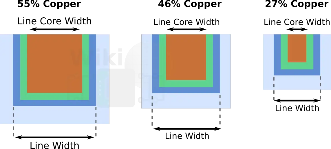
From the table above it can be seen that copper has considerably lower resistivity than aluminum, tungsten, and cobalt. So why switch? Electromigration. The high-speed electrons that flow through the wire occasionally bump into the copper ions causing a momentum transfer, gradually skewing them in a certain direction. Using a pipe analogy, the metal density at one end decreases and piles up on the other end. The decreased density, or void, affects the reliability of the integrated circuit which eventually results in a failure due to the increased resistance.
To mitigate the problem and protect the wires, manufacturers introduced diffusion barriers and liners using other materials such as silicon/tantalum nitride and oxynitride. The barrier is used to to prevent metal diffusion into the dielectric while the liner is used as “glue” for the barrier and the copper. Once those are in place, the copper seed layer (metal plating) and then the bulk copper is added.
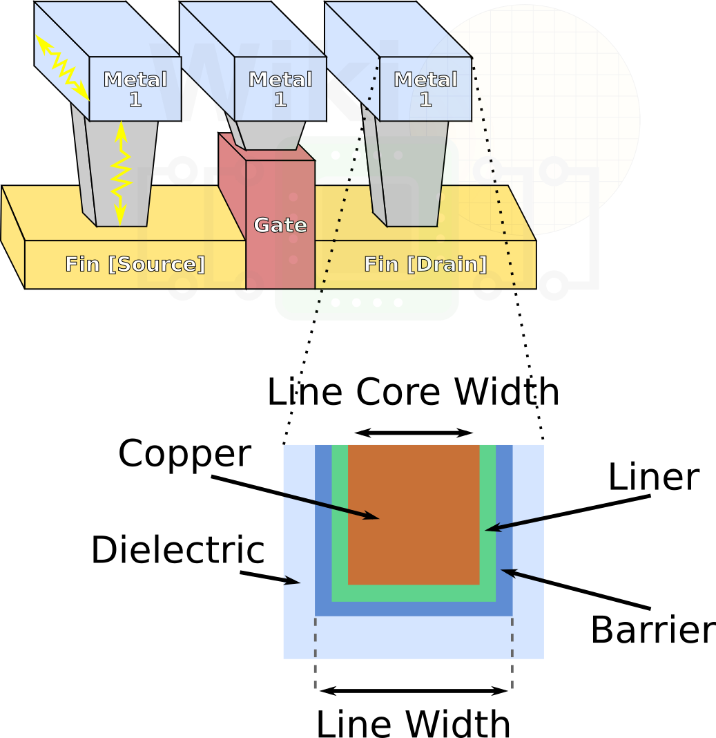
This worked nicely, but there is a problem. As interconnect continued to shrink, the thickness of the high-resistivity liner/barrier for the copper interconnects stayed more or less the same. This is largely due to the difficulty in thinning it any further than the few nanometers it already is. This means that as the wires scale, the barrier itself takes up a larger and larger portion of the interconnect cross-sectional area. With the high-resistivity barriers slowly making up a larger portion of interconnect, it begins to dominate the resistivity of the wire itself.
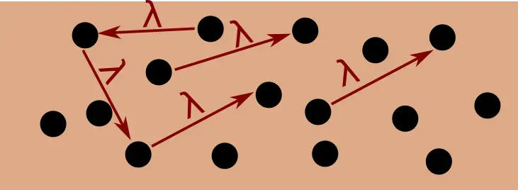
This isn’t the only issue affecting the wire scaling. The mean free path is the average distance the electron travels between collisions. Since the mean free path λ for copper is almost 40nm, then as the copper interconnect approach λ or 40nm, the copper electrons will begin to scatter far more often from the various surfaces and grain boundaries because they are so area-constrained. This excess scattering increases the resistivity of copper.
So while the transistor performance has been improving, the copper wire resistance has actually been increasing as the wire got smaller. This means that the signal slows down, distance traveled decreases, and we’re consuming more power than desired. In other words, despite having higher performance transistors, there is a growing disparity between the transistor capabilities and the wire capabilities. The copper wires have become a serious bottleneck.
Cobalt on the other hand has higher resistivity, but its electron mean free path is considerably lower – in fact it’s 1/4 the average distance, down to single-digit nanometer. Additionally, in contrast to copper, it has been demonstrated that a single film, as thin as 1 nm, is sufficient to serve as both the liner and barrier for cobalt. This creates a new scaling path forward for cobalt interconnect. While there are a couple of other factors that determine the final resistance of the wire, it looks as though Intel has managed to hit the Copper-Cobalt Crossover point whereby cobalt results in a performance win over copper. We suspect foundries will follow Intel as they scale their interconnects in future nodes.
It’s worth noting that cobalt isn’t used for everything. It’s only used for the first two metal layers (i.e., M0 and M1) where you have your local interconnect that have very narrow pitches (e.g., 36nm) and where cobalt does benefit them. Intel claims this provides a 2x reduction in via resistance as well as 5-10x improvement in electromigration in those layers. For the global routing and the large power rails which are longer distance and much thicker, it makes sense to continue to use copper. With future nodes, as additional upper metal layers shrink below the Copper-Cobalt crossover point, we’ll start to see cobalt climbing up the stack.
In addition to interconnect, Intel is also using cobalt for the Metal 2 through Metal 5 cladding layer to also improve electromigration. Low-κ carbon doped oxide (CDO) dielectrics are used on eleven layers out of the thirteen. This is the same Low-κ that was used for the 14 nm process. Finally, Intel also introduced cobalt fill at the trench contact, replacing the tungsten contact metal which was used previously (note that tungsten is continued to be used for the gate) due to the narrow line widths, reducing resistance.
–
Spotted an error? Help us fix it! Simply select the problematic text and press Ctrl+Enter to notify us.
–