
IEDM 2017 + ISSCC 2018: Intel’s 10nm, switching to cobalt interconnects
Air Gaps
At the 14nm node, Intel became the first to introduce air-gaps into logic devices high volume manufacturing. Air gaps were used in order to improve the capacitance at the two performance-critical local interconnect layers. The air gaps provided 17% improvement in capacitance.
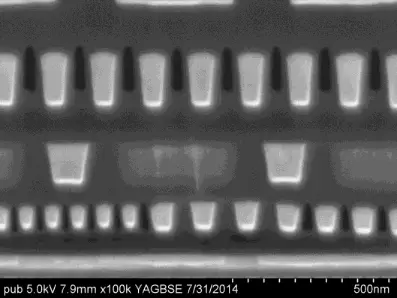
Air gaps were not mentioned during their 10nm IEDM presentation, but we did get a chance to ask about it after. While air gaps were not used for the design presented in their paper, Mr Auth noted that air gaps are definitely an option in their 10nm, it’s currently just a matter of cost. For each layer you add air gaps to, you have to add another mask. It’s entirely possible we’ll see it make an appearance as the process matures.
EUV
At IEDM Britt Turkot was invited to talk about EUV lithography. Extreme Ultra-Violet (EUV) lithography has an exposure wavelength of 13.5nm, very close to the soft X-rays area of the electromagnetic spectrum. EUV thus offers a very attractive alternative to the current deep ultra-violet (DUV) 193nm-immersion lithography being used by improving resolution and reducing Edge Placement Errors (EPEs). The development of EUV lithography has been excruciatingly slow. There are a large number of different things that must come together for EUV to enter mass production – resist materials must satisfy the resolution targets with acceptable Line Edge Roughness (LER), the exposure source must provide adequate power, and the reticle defect inspection must greatly improve. Sufficiently high power isn’t enough, it must be done with high availability in order to meet the demands of high-volume manufacturing.
Exposure power improvements has historically been plagued with delays. Turkot reported that recent advances in Laser Produced Plasma (LPP) technology over the last few years has allowed exposure sources to reach power levels sufficient to support HVM, however they also remain the largest contributor to exposure system downtime and availability.
EPE improvement from EUV relative to 193nm immersion lithography is anywhere from 33% to 90% for various via feature geometries. Those improvements are a result of EUV’s higher effective contrast and elimination of pattern placement errors due to consolidation of multiple masks.
In order to create defect-free EUV masks, defect repair technologies have been developed including cutting repair and patching repair. As the name implies, cutting repair involves removing portions of the unintentional absorber material while patching involves adding an absorber material in order to compensate for a defect. Turkot has reported that using combination of pattern shifting along with mask repair, Intel Mask Operations has successfully produced multiple EUV masks with zero printable defects.
In the area of pellicle, significant advances has been made by ASML with pellicle mounting and support tooling being made available to customers. In order to detect defects, there is a large push for Actinic Patterned Mask Inspection (APMI). Intel noted that while the current lack of commercial APMI is not a show-stopper, yield and cost could become an issue.
All in all, Intel is confident that EUV is on a solid path to HVM insertion, however Turkot was careful to note that insertion will only take place when the technology is ready and cost effective. We believe Intel will insert EUV in late 2019/early 2020 in preparation for their “10nm++” 3rd generation enhanced process.
Final Thoughts
The monumental engineering feat Intel has presented at IEDM 2017 can only be described as a highly advanced 7nm-class manufacturing technology. Interestingly, if they ramp-up by around mid-year, they will still manage to squeak by and maintain 7x density in roughly 7 years in their relentless pursuit to keep Moore’s Law going. So far it has worked and while Moore’s Law is still alive, it’s becoming ever more difficult to pursue.
Unfortunately, this isn’t being done in a vacuum and while their 10nm was initially supposed to ramp-up in late 2016, it has since shifted to 2018. During that time, their competition such as TSMC has managed to release their 10nm process.
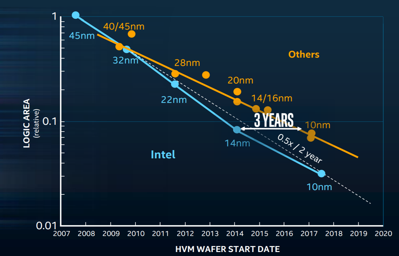
Both TSMC and Samsung 10 nanometer nodes are more comparable to Intel’s 14nm, however, Intel’s 10nm delays which has lasted throughout 2017 has meant that their competitors have managed to further narrow the gap dramatically. TSMC will ramp-up their 7nm production sometimes later this year and GlobalFoundries will follow sometimes in late 2019. Unlike foundry 10nm nodes, their 7nm nodes are in fact more or less comparable to Intel’s 10nm in terms of density. While Intel still leads with various advances to the wiring such as the aggressively scaled cobalt local interconnections, they no longer have a multi-year density lead.
2019 will be the first time in a fairly long time that all four leading-edge foundries (Intel, Samsung, TSMC, and GlobalFoundries) will be on an even playing field. Ultimately it’s not our analysis, but the final products, that will demonstratively prove what those process technologies have to offer and who is leading the semiconductor industry.
–
Spotted an error? Help us fix it! Simply select the problematic text and press Ctrl+Enter to notify us.
–