
IEDM 2017 + ISSCC 2018: Intel’s 10nm, switching to cobalt interconnects
Device Architecture
This is Intel’s 3rd generation FinFET. They first introduced FinFET at the 22 nm node, a generation ahead of the foundries and has since undergone some fairly significant modifications.
Fin
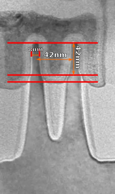
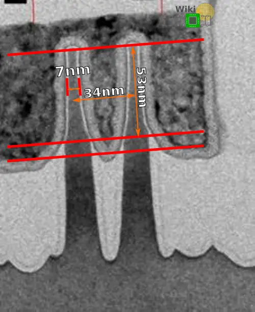
As you scale you want the fin width to get narrower in order to improve the short channel characteristics and subthreshold slop but it also degrades the external resistance. For their 10nm, Intel uses a 7nm fin width at the middle of the fin height.
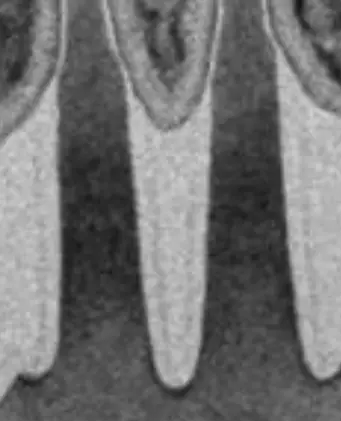
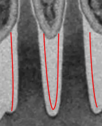
As you scale, you also want the fin to be taller in order to increase the drive current but it also increases the stray capacitance and gate capacitance. For their IEDM presentation, Intel presented a device with a 46 nm fin height but the accompanying TEM image has a much taller fin. Their 10nm transistors can vary from roughly 43 to 54 nanometers tall. Intel has stated that this is a variable that they can optimize by product depending upon the power and performance needs of that particular product. Mr Auth also stated that they can actually go further with additional optimizations but this simply isn’t necessary for their products for the base process.
The last vector you want to adjust as you scale is the fin pitch. You want the fin pitch to be tight in order to reduce the parasitic capacitance. At the smaller pitch dimensions, this becomes a pretty complex task due to the patterning complexity involved as well as for the dummy gate and workfunction material insertion. For their 10nm process, Intel uses a fin pitch of 34 nanometers which does require self-aligned quad patterning (SAQP). Basically you start with two sacrificial layers and pattern the first layer with a 136-nanometer pitch. You then deposit and etch the spacer and then remove the first sacrificial layer and etch into the second sacrificial layer which will give you a 68-nanometer pitch. You then deposit and etch the second spacer and remove the second sacrificial layer and etch in the fins and remove the second spacer which will result in the quarter of the original pitch (i.e., the desired 34 nm pitch). Versus self-aligned dual patterning (SADP) this only adds four additional steps (three etch, one deposition steps, and no extra lithography steps).
| Fin Comparison | |
|---|---|
| 14nm | 10nm |
 |
 |
| Source: Intel, IEDM 2017. | |
The end result is tighter, taller, and straighter fins which provides better short-channel characteristics, better drive current, and better matching.
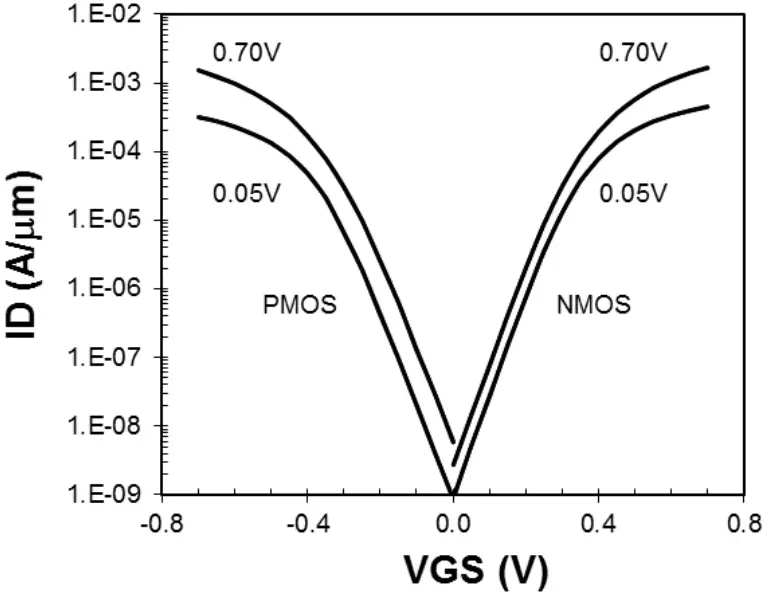
Both for nMOS and pMOS transistors Intel demonstrated a steep subthreshold slopes of 70 mV/dec and low DIBL of ~70 mV/V for the minimum device size of 18nm Lg.
The minimum gate length was reported at 18 nm with a 54 nm gate pitch. This is their 7th generation strain silicon with a stresser being used for both the pMOS and nMOS. With this process, Intel has introduced a new first interlayer dielectric (ILD0) layer stresser through the gate, orthogonal to the fin which they used to enhance the drive current on the nMOS transistor (Interestingly, the paper says by 5% but at IEDM he reported a higher value so we presume this was enhanced further after the paper was submitted). Additionally, the source and drain epis are in-situ doped to provide lower contact resistance.
In their 22nm node Intel started using low-κ spacers. As you scale the gate pitch, the space between the contact and the gate continues to get constrained which in turn means the spacers continue to get smaller. This means the parasitic capacitance between the contact and the gate is slowly becoming a larger contributor to the overall performance of the transistor. For 10nm Intel is using a spacer with a lower-κ value which they claim has reduced the capacitance by 10% (compared to the previous spacer, this is a 78% reduction in capacitance).
Intel has four workfunction metals for their base process and another optional six workfunction metals, allowing them to use whichever one they need tailored to the end product goals. This allows them to run undoped channels throughout the entire Vt range (i.e., standard Vt but also for low and high Vt devices).
 |
 |
Contacts
The contacts area has also been greatly enhanced. 10nm continues with the self-aligned contacts. As you scale the gate pitch, the contacts continue to get smaller which impacts the contact resistance of the diffusion trench contacts to the source/drain region and in the case of local interconnects it also impacts the strain resistance. Intel has switched from tungsten to using cobalt for the trench contacts themselves which is said to provide a 60% reduction in contact line resistance and roughly 1.5x reduction in contact resistance. They have also added a conformal titanium layer to wraparound the source/drain diffusion regions. Additionally, they have added a thin NiSi layer on the pMOS epi to lower the contact resistance.
Drive
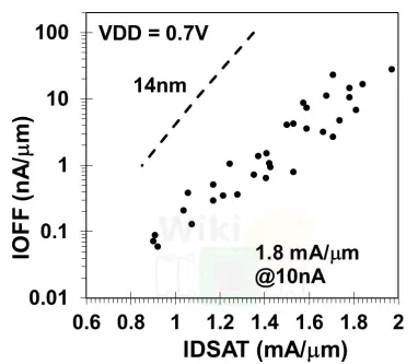
All in all, the massive amount of engineering has resulted in significant performance. The combination enhancements leads to a nMOS drive current of 71% over their 14nm with a drive current of 1.8 mA per micron at a supply voltage of 0.7 V and an Ioff of 10 nA per micron. Likewise, the nMOS IDLIN is 0.475 mA per micron, an increase of 100% compared to 14nm FINFET transistors.
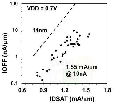
For pMOS, Intel showed a drive current of 1.55 mA per micron at a supply voltage of 0.7 V and an Ioff of 10 nA per micron which is 35% improvement over their 14nm with a 55% improvement in the pMOS IDLIN which is at 0.325 mA per micron.
| 10nm Drive Current Improvement over 14nm | ||
|---|---|---|
| Device | IDSAT | IDLIN |
| nMOS | +71% | +100% |
| pMOS | +35% | +55% |
Since the capacitance at 10nm makes up a larger portion of the transistor performance, Intel reported on a ring oscillator performance they’ve designed as a metric. At the nominal voltage of 0.7 V, the performance was shown to be 20% higher than the 14nm version for the same leakage.
To test the performance of their SRAM, Intel designed a 72 Mb SRAM test die which showed the median active Vcc min was 0.56 V.
–
Spotted an error? Help us fix it! Simply select the problematic text and press Ctrl+Enter to notify us.
–