
Intel Launches Lakefield: An Experiment With Multiple New Technologies
Although originally planned for late 2019, Intel is finally shipping the first few models based on the Lakefield SoC. The new chips mark the beginning of a new experiment involving several new technologies. Lessons from these technologies will undoubtedly find their way in improved forms in future Intel products.
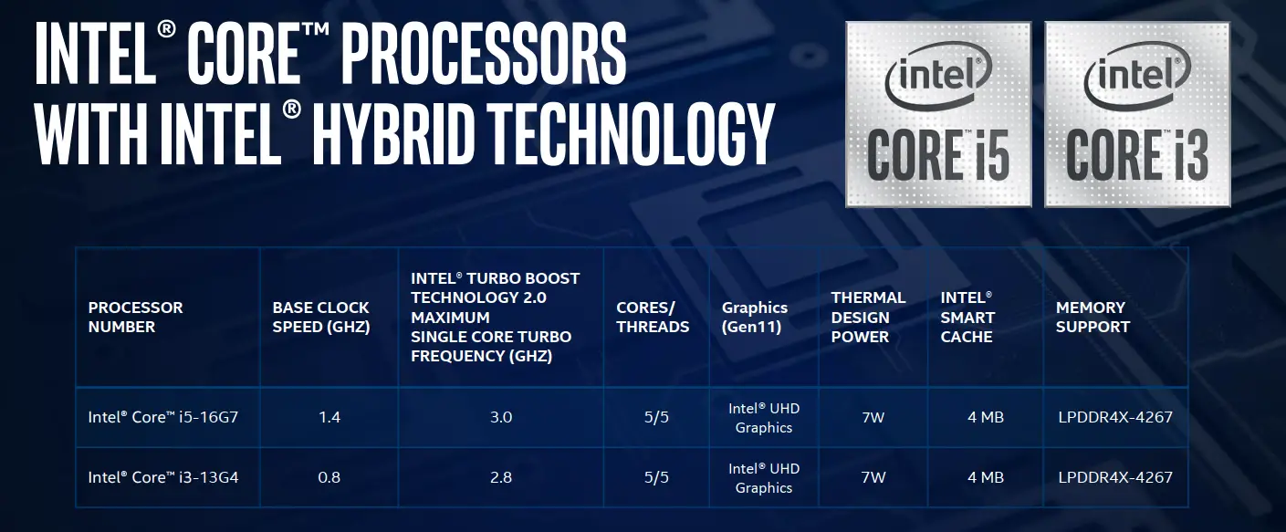
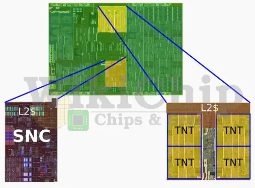
Two new models are launching today – Core i3 and Core i5. In terms of CPU specification, both models are identical – only differ in frequency and thus overall performance. Both processors feature Gen11 GPU, however, the Core i3 includes 48 execution units while the Core i5 features the full 64 EUs enabled. Both SoCs offer five cores consisting of a quad-core Tremont small-core cluster and a single big Sunny Cove core. Note that the Sunny Cove core does not support hyperthreading on Lakefield.
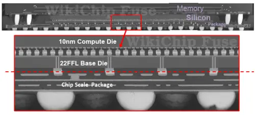
Both models target a TDP of 7 W putting it at just about the maximum possible for fanless devices. These chips also come with 8 GiB of LPDDR4x-4267 POP memory packaged. The two chips come in a flip-chip chip-scale package (FC-CSP) measuring 12x12x1 millimeters.
| Lakefield Models | ||||||||
|---|---|---|---|---|---|---|---|---|
| Model | Cores | Base | Turbo | Graphics | ||||
| 5C | 1C | EUs | Base | Burst | ||||
| Core i5-16G7 | 5 (5T) | 1.4 GHz | 1.8 GHz | 3.0 GHz | 64 EU | 200 MHz | 500 MHz | |
| Core i3-L13G4 | 5 (5T) | 0.8 GHz | 1.3 GHz | 2.8 GHz | 48 EU | 200 MHz | 500 MHz | |
There’s currently no i7 part. It’s entirely possible as binning gets better and there is demand, we’ll see a new “i7-L17G7” or something similar with a slightly higher base and turbo frequencies.
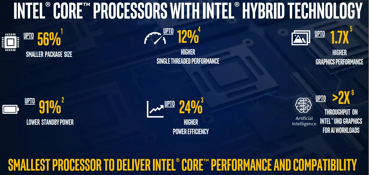
Intel’s website suggests both SKUs have a recommended price of $281. Given this is an OEM product, the actual price is much lower. If the RCP on the website is correct, it suggests that Intel is aggressively pricing these products. Consider the top-end Amber Lake SKU – the Core i7-8500Y – which has an RCP of $393. That’s $112 cheaper while being objectively better at just about everything. And that includes the 8 GiB of POP memory which is already inside the package, eliminating it from the OEM BOM entirely. The i7-8500Y is the SKU Intel is using to make its comparison in the slide below. It’s a great comparison point given they both target the same premium ultra-mobile device market with similar specs (albeit an older architecture) and TDP (5 W with cTDP of 7 W).
The 8500Y is a dual-core microprocessor with 24 EUs from the Gen9.5 GPU architecture. Like Lakefield, the 8500Y integrates the chipset on-package albeit not 3D stacked. The 8500Y has 2 Skylake-class CPU cores with multi-threading whereas Lakefield has a single Sunny Cove core without multithreading along with 4 Tremont cores. If we were to try to make an apples-to-apples comparison, it should be comparable to slightly higher-performance three Skylake-class cores, apart from some vector extensions. Compared to the 8500Y, Intel claims the new Lakefield models are able to achieve up to a 91% reduction in standby power. In terms of power-efficiency, on benchmarks such as the WebXPRT 3, they are reporting up to 25% higher score per watt. Since Lakefield incorporates a Sunny Cove core, in terms of single-thread performance, Intel says SNC can deliver a 12% higher score on SPEC CPU2006. On the graphics side, the performance should also be noticeably better. With the i5-16G7 incorporating 64 execution units. That’s 2.67x the EUs on the 8500Y. Therefore despite the lower burst frequency, there should be a significant uptick in performance.
An Experiment
Beyond the value proposition to customers, Lakefield is significant for the technologies it’s introducing and the challenges they are bringing along.
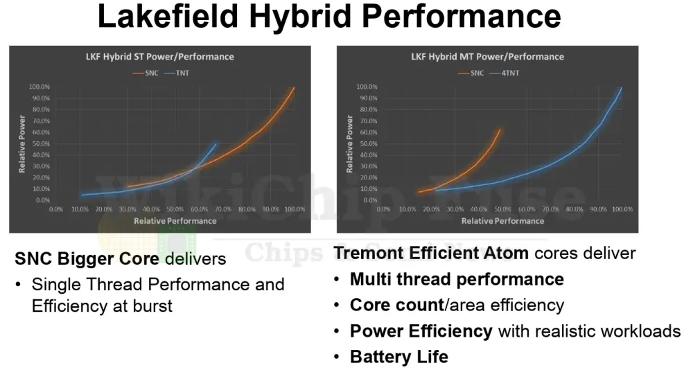
Although heterogeneous multi-core chips aren’t new in the mobile space, they are new in the x86 space. Lakefield is the first x86 product shipping with two entirely different core architectures. The motivations are very similar to Arm’s big.LITTLE architecture, workloads that can leverage high throughput will enjoy higher power efficiency from slimmer power-efficient cores versus large big cores that target peak performance. Likewise, for complex workloads, a beefy OoO core can deliver that higher performance when desired. The motivation, at least in theory, should also work well for other types of products such as a server part that offers both high single-thread performance and high-throughput performance. Lakefield differs a bit from Arm’s traditional big.LITTLE architecture in the fact that the Tremont cores are by no means “little” (e.g., A55). They are highly capable out-of-order cores. They do, however, offer much better performance/power versus Intel’s large cores, albeit while falling of their peak performance.
Beyond the hardware, advanced scheduling is needed to do this well. It will be interesting to see how well Windows is able to migrate workloads based on the feedback the SoC provides. If Intel hopes to use the technology in a broader portfolio of products, getting this right is essential. That being said, sacrifices were made in Lakefield. In order to simplify process migration, both the Tremont cores and the Sunny Cove core were reduced to the lowest common denominator with symmetric ISA support. This means no AVX, AVX2, and AVX512 support on the Sunny Cove core (one of the big advantages of the Sunny Cove cores in Ice Lake). While it makes migrating workloads between cores simple, it misses out on many of the fantastic vector instructions that were introduced over the last decade.
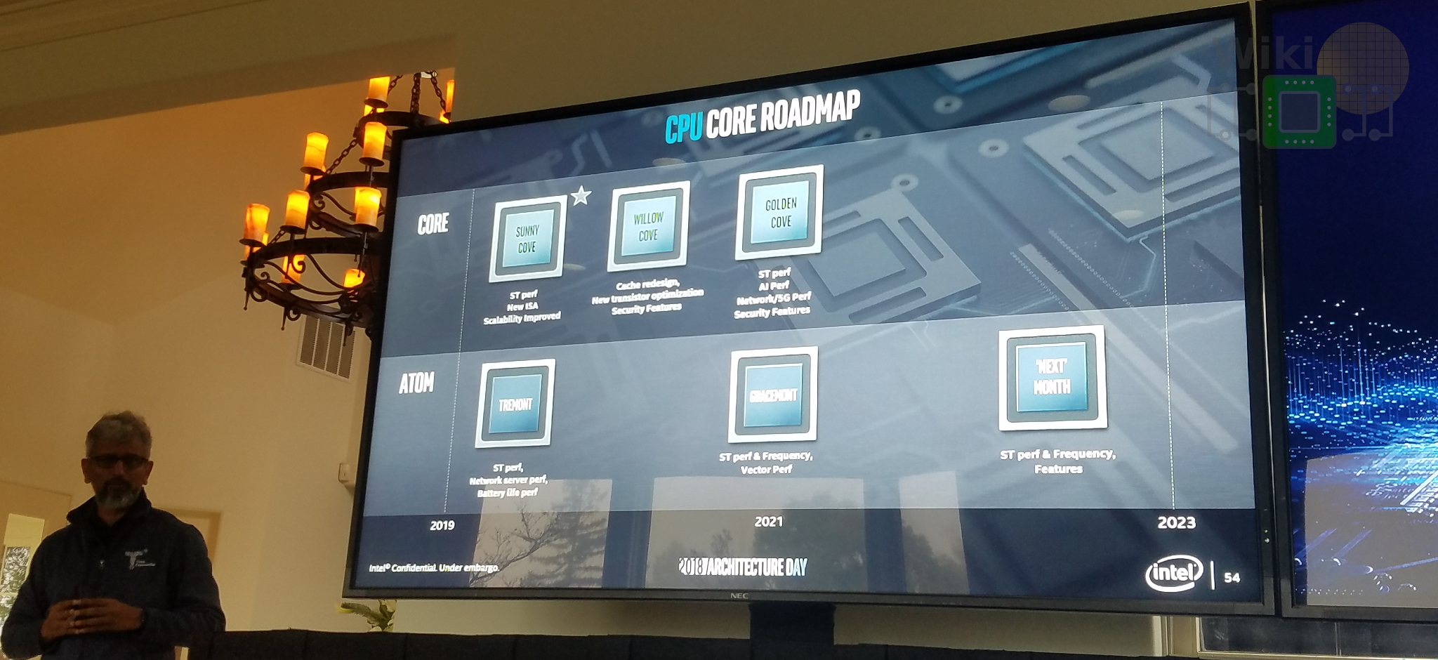
In an HPCA paper from 2009 nonetheless [Li, et al. HPCA-16 2010], Intel proposed a number of algorithms and enhancements to the operating system that would allow heterogeneous cores with overlapping, but non-identical instruction sets to work correctly. Such support could make future Lakefield chips support both up to SSE 4.1 on the small cores while offering the full AVX512 support on the big cores. In Intel’s 2018 Architecture Day, one of the roadmap bullet points mentioned for the successor of Tremont, Gracemont, is “Vector Performance”. Vector performance could mean many different things and mong the possible choices is AVX support. Introducing AVX on the small cores is a bit of odd choice but it would upgrade the ISA support for all the cores to whichever AVX extension they choose to support.
No large vector support on Tremont is part of the reason the cores take up so little silicon area. In fact, on their current design, the entire Tremont cluster is almost the same size as a single Sunny Cove core. A quad-core Tremont cluster should be close to or comparable to the integer performance of a quad-core Haswell group while offering much higher power-efficiency. Those are pretty good PPA numbers. Lakefield’s entire compute die is just 82 mm² packing 4.05B transistors on their latest 2nd-generation (10nm+) process.
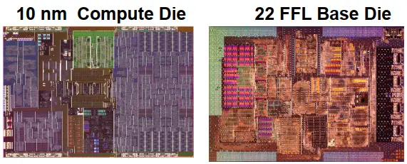
Lakefield packaging is another first. The chip utilizes Intel’s Foveros technology to 3D-stack the compute die to the base die. While the compute die is fabricated on 10nm+ in order to take advantage of the company’s latest high-density high-performance transistors, the base die is fabricated on 22FFL.
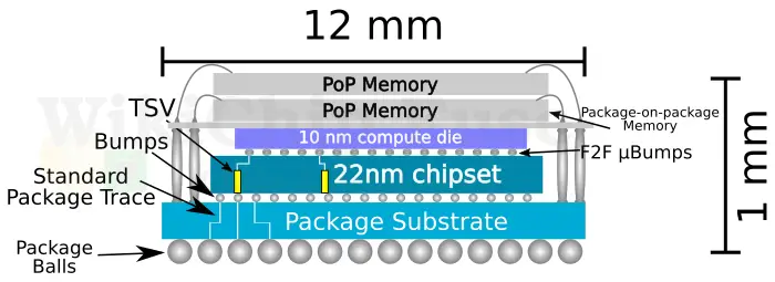
22FFL is Intel’s cost-sensitive lower-power process they can use to fabricate much of the standby logic and other analog I/O circuits that could benefit from the low-leakage transistors. In Lakefield, for example, all the PCIe PHYs have been moved from the compute die to the base die. The base die on Lakefield is slightly larger than the compute die, measuring just 92 mm² and packing 650 million transistors.
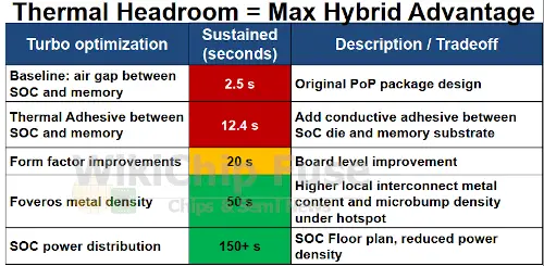
Thermals present a big challenge in 3D stacking. No product is immune, not even Lakefield at just 7 W. If we are to see 3D stacking introduced in high-performance applications, optimizing for better thermal removal will be essential. That being said, Lakefield already introduced a number of optimizations in order to help with thermal removal. Given Lakefield has the compute die effectively sandwiched between the POP memory and the base die, ensuring that heat can efficiently escape the compute die is important. Among the techniques, Intel introduced a new thermal adhesive flow designed to eliminate the air gap between the compute die and DRAM memory. Additionally, a lot of physical design work went into ensuring there is proper mitigation for hot spots. Thick metal layers were also used to improve the thermal conductivity and spread the hit over hot spots. We expect to see more of this sort of optimization on both the packaging and silicon in order to improve the thermal headroom of future devices.
Products
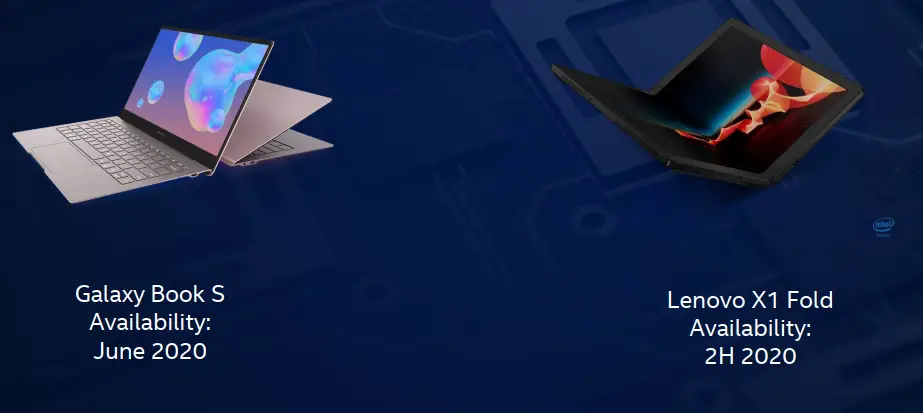
At least two new devices have been announced. The Samsung Galaxy Book S which should be available starting this month and the Lenovo X1 Fold which is expected to launch in the second half of the year.
Related Articles
- A Look at Intel Lakefield: A 3D-Stacked Single-ISA Heterogeneous Penta-Core SoC
- Intel Unveils the Tremont Microarchitecture: Going After ST Performance
- Intel Looks to Advanced 3D Packaging For More-than-Moore to Supplement 10- and 7-Nanometer Nodes
–
Spotted an error? Help us fix it! Simply select the problematic text and press Ctrl+Enter to notify us.
–