
Intel 2021 Process Technology Update: Intel 7, Intel 4, Intel 3, and Intel 20A
Today Intel held its global Intel Accelerated event where the company revealed a detailed process and packaging technology roadmap for the next half-decade. At the event, the company outlined its upcoming process technologies for the next couple of years.
This article is part of a series of articles covering Intel’s 2021 Accelerated Event:
- Intel 2021 Process Technology Update
- Intel Announces 20Å Node: RibbonFET Devices, PowerVia, 2024 Ramp
- Intel Unveils Foveros Omni And Foveros Direct; Leveraging Hybrid Bonding

Updating The Node Names
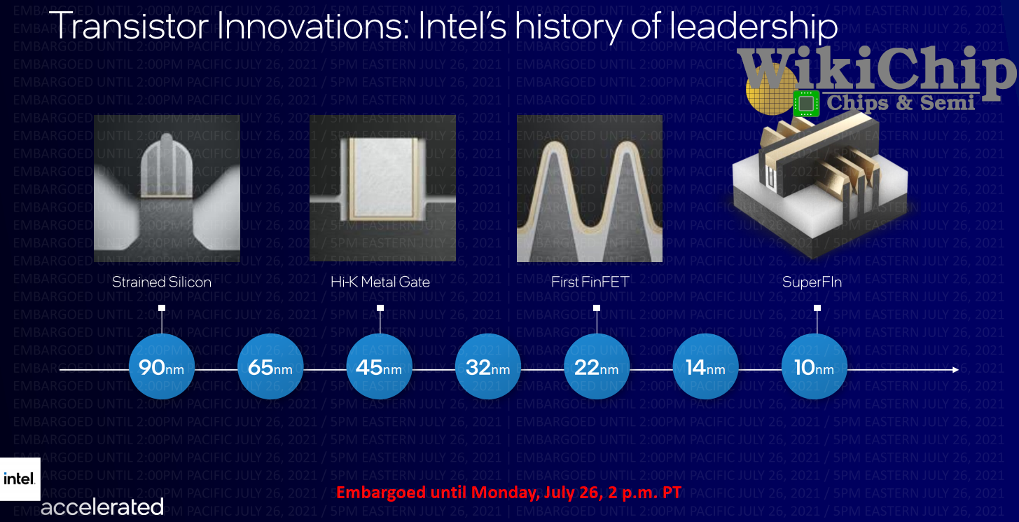
Node names over the past half-decade have grown into a hotly debated topic. This is partially due to the names not really reflecting any measurement of the transistor, but it’s also largely due to the disparity in the meaning of the node names between Intel and the other foundries – primarily Samsung and TSMC. For example, when comparing Intel’s 10-nanometer PPA, we’ve long noted that it’s far more comparable to Samsung and TSMC’s 7-nanometer node than to their 10. In fact, area scaling-wise, Intel’s 10-nanometer high-density standard libraries are slightly ahead of foundry 7-nanometer. It’s no surprise that Intel has been struggled to convey to the more general public that their 10-nanometer is as good or better than foundry 7-nanometer (and 7 vs foundry 5/6). Going forward, Intel is renaming its process technologies in order to better align the process characteristic with foundry nodes. While we don’t quite agree that an actual process node renaming is necessary, Intel has chosen to rebrand some of its nodes to better reflect their PPA versus other foundries. It’s also worth noting that since Intel is now doubling down on its Intel Foundry Services as part of its IDM 2.0 strategy, node names have gained a slightly more important role given the fact that external customers are now potential users of those nodes.
The renaming is taking effect from future nodes only – starting with their upcoming 10-nanometer Enhanced SuperFin. Prior process nodes will remain unchanged to avoid confusion for already shipping chips. So for example, Tiger Lake, which is shipping on Intel’s 10nm SuperFin will remain unchanged. As part of the renaming, what were previously ‘notelets’ such as 7nm+/++ now have their own name to reflect it similar to how other foundries have named their (e.g., 8nm, 6nm, and 4nm).
10-nanometer Update
Intel 10-nanometer problems plagued the company for nearly half a decade. Today Intel made it crystal clear that 10-nanometer is working. This is important because although incredibly late and behind, the common belief among industry watchers has been that it’s not working as it should (either not meeting the performance or not yielding). At today’s event, Dr. Ann Kelleher, senior vice president and general manager of Technology Development, drilled down on the state of their 10-nanometer node. Kelleher reaffirmed that 10-nanometer production has ramped up and is in high volume at three factories in Oregon, Arizona, and Israel. “Furthermore, our volume production has crossed over. This means we are manufacturing more 10-nanometer wafers than 14-nanometer wafers. In short, 10-nanometer is doing really well,” she added.
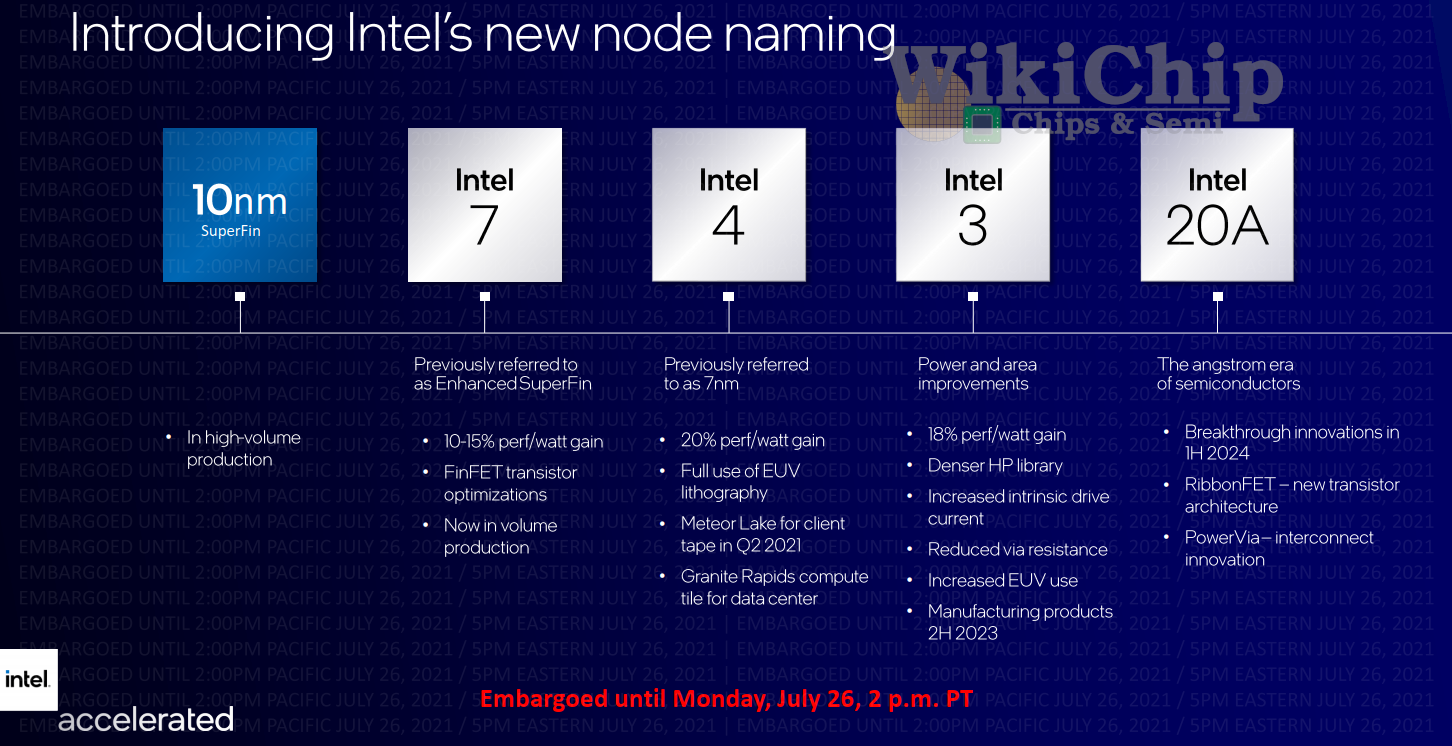
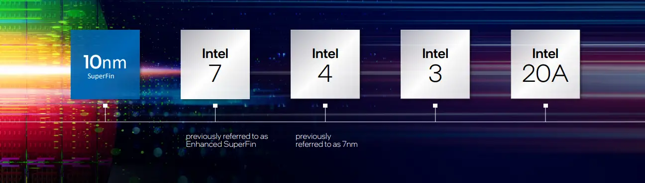
10-nanometer Enhanced Superfin -> Intel 7
As we noted previously, Intel is only rebranding future process nodes and that means starting with Intel’s upcoming 10-nanometer Enhanced SuperFin technology. Intel’s 10 nm Enhanced SuperFin will now go under the new “Intel 7” (no “nm”) moniker. Although it’s an enhanced version of the prior 10-nanometer node, Intel 7 does bring in some sizeable improvements – on the order of a full node improvement in terms of energy effiency. Intel says that the Intel 7 offers 10-15% performance-per-watt improvement over the prior 10-nanometer SuperFin technology. “This is equivalent to a full node of performance gain. As a result, we believe, that Intel 7 is an appropriate name to help customers understand the kind of competitive performance being delivered by the name” Kelleher said.

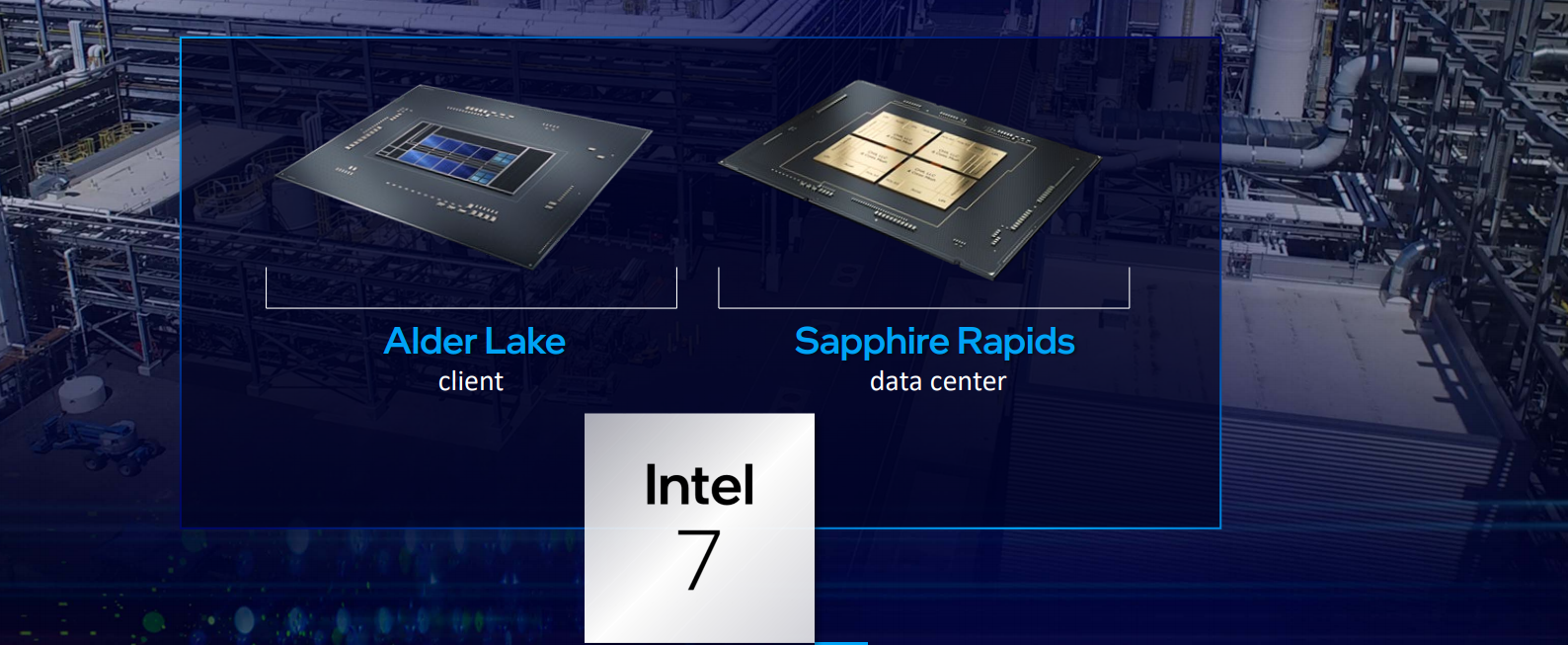
Intel 7 performance is achieved through higher strain transistors, better energy control, and improved power delivery and metal stack. Intel says the process has entered mass production and will be used for the company’s upcoming Alder Lake client processors which are expected to launch later this year and Sapphire Rapids data center processors which will launch in the first quarter of 2022.
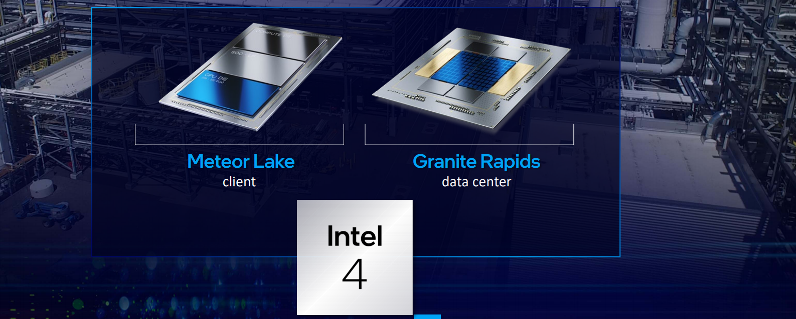
Intel 4
Intel’s next major node which used to be called “7 nm” is now being called “Intel 4” to better reflect how their node compares to other foundries’ technology. Intel 4 will offer a 20% performance/watt gain at a fixed power (for products that rely on the power reduction aspect of the node, the improvements are greater). Intel 4 will utilize an optimized FinFET device technology like prior nodes and will be ready for mass production in the second half of next year. Intel 4 is Intel’s first process node to fully embrace EUV technology which is said to considerably simplify their process. Intel 4 will utilize EUV for up to twelve layers.
Earlier this year the company mentioned that they have addressed the initial issues they had with the process. “In March we told you had put the previous issues with this process node behind us. I think it’s important that we spell out what that means. First, we hit an important milestone when we taped in the Meteor Lake client compute tile last quarter. Beyond the actual wafer, we are right where we expect to be relative to our performance and defect density expectations. Indeed, our defect density trends is on the right path to meet our product commitments,” Kelleher noted.
Intel says its lead production for Intel 4 will be Meteor Lake for the client market which has taped in in the second quarter of this year. For the data center, Intel Granite Rapids compute tile will also be fabricated on this node. Both products will be shipping in the first half of 2023.
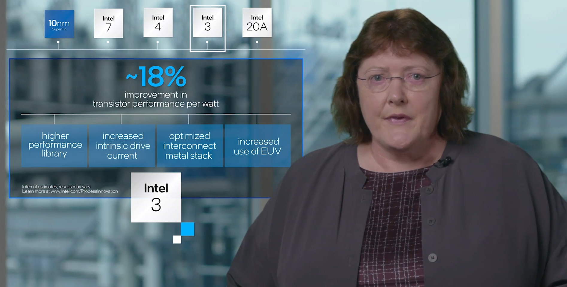
Intel 3
Intel 3 is the next follow-up node. This node will also be a foundry node as part of Intel Foundry Services. Presumably, this was previously called “7nm+” or “7nm++”. Intel 3 will be the last leading-edge process technology by Intel to utilize FinFET devices. This technology is said to offer roughly 18% improvement in performance/wall with higher power reduction numbers at a fixed performance.
Intel 3 will offer a new denser high-performance (HP) standard library that will offer greater area scaling. Although they did not go into great detail, Intel says that the node will offer further via resistance improvement, possibly through new material or techniques along with an optimized interconnect metal stack. As with Intel 4, Intel 3 will also make extensive use of EUV technology beyond Intel 4. “This is a higher level of improvement than a standard full-node improvement for us.”
Intel 3 will enter production in the second half of 2023.
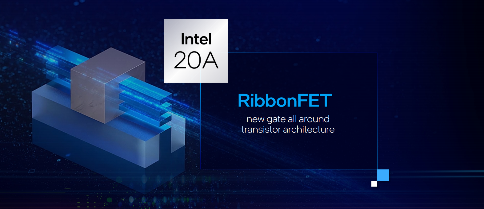
Intel 20A
Intel 20A is the next major node which includes a new transistor architecture and a number of other major process changes. We have a separate article that covers some of the new details that were disclosed.
2025 And Beyond
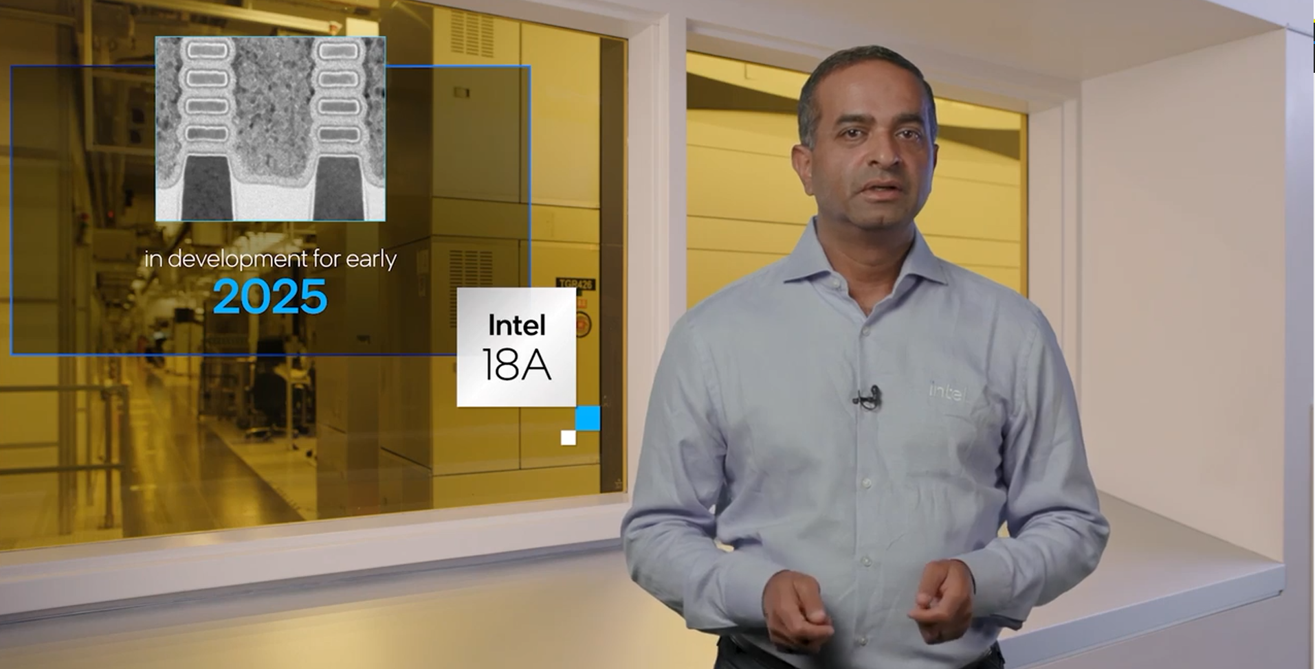
Beyond 20A, Intel has Intel 18A node in development. Although they are not ready to disclose too much information on this node, the company says 18A will make use of a refined version of their RibbonFET and will deliver another major jump in transistor performance. 18A will also utilize ASML’s high-NA EUV steppers. Intel says it expects to receive the first production tool in the industry for this process.
Intel is targeting 18A for early 2025.
First to High-NA
Intel’s slower move to EUV meant that the company relied on complex multi-patterning techniques to achieve similar results using conventional 193i tools which is a major reason for their 10-nanometer woes. At the event Kelleher addressed this, saying “as EUV evolves, Intel plans to adopt the latest tools as soon they are made available. This ensures our fabs have the latest features from ASML to deliver the highest productivity in support of our technology requirements. Ramping EUV into volume requires an entire ecosystem surrounding the equipment – photoresist, mask generation, pellicle production, and metrology. We have put a great deal of effort into building this ecosystem. In fact, Intel’s IMS subsidiary is the primary supplier of EUV multi-beam mask writers worldwide. These tools are essential for creating high-resolution masks which are a critical part of enabling EUV lithography. This mask-writing technology is a competitive advantage for us as well as a key enabler for the industry. We are working together to also define, build, and deploy next-generation of EUV tools – referred to high-NA EUV.”
To that end, Intel says it expects to receive the first production high-NA tool in the industry and intends to be the first to implement high-NA in production beginning in 2025.
–
Spotted an error? Help us fix it! Simply select the problematic text and press Ctrl+Enter to notify us.
–