
Left, Right, Above, and Under: Intel 3D Packaging Tech Gains Omnidirectionality
As the industry heads into the 2020s, advanced packaging will not only become a necessary tool for compensating for the diminishing benefits of process scaling, but they have the potential to provide unique and distinct advantages to companies with such capabilities. A number of companies are the forefront of this transformation. Previously we reported on TSMC’s effort which includes CoWoS for high-end performance-demanding applications, the extensive family of InFO packaging flows, and their SoIC demonstration of 3D IC stacking. Likewise, Intel’s portfolio of advanced packaging includes their 2.5D EMIB and the face-to-face 3D stacking Foveros technology. More recently, the company added Co-EMIB which combines the two into a more complex chip.
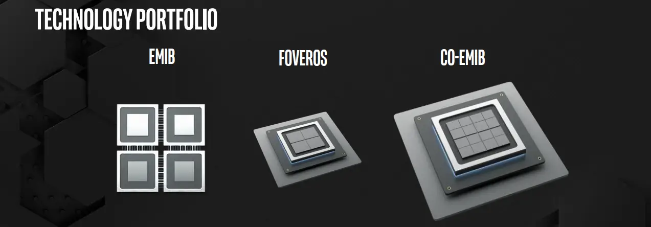
The Embedded MultiInterconnect Bridge (EMIB) has several fairly clear advantages over traditional silicon interposer. Embedding a small piece of silicon where needed over a large interposer has a clear cost advantage. First-generation of EMIB products have been shipping for some time in a number of products including the company’s high-end Stratix X FPGAs and in Kaby Lake G mobile chips. By early last year, Intel shipped over a million EMIB-based products. Although those are ultra-premium products and thus not quite as high volume as they would like in order to amortize the cost of the technology, it’s enough to improve on the technology as it starts shipping in more products. Like EMIB, Foveros provides an even more significant increase in bump density but it does this by stacking two dies directly face-to-face which comes at a higher cost.
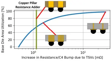
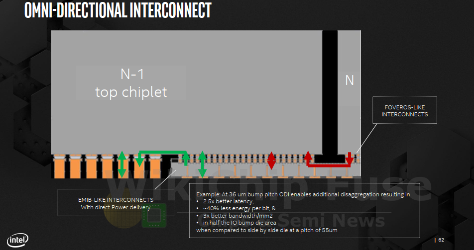
Both EMIB and Foveros have their advantages, but they are far from perfect. Consider Foveros for example which offers very high bandwidth between the top and bottom dies. In order to bring power to the top die, vias have to be dropped through the bottom die. TSVs add resistance and while that can be mitigated by adding more vias, it incurs additional area costs. On top of that, keep out zones and the inherent addition to the existing routing congestion exacerbate the situation. According to Intel, a conservative estimate is in the ballpark of a 20% die area increase. In certain situations that can be as high as 70%. And then there is the issue of thermals. For high-performance applications, heat removal is a major concern as the top die increases the thermal resistance by obstructing the path to the heatsink. Traditional silicon interposers avoid this problem by spreading the dies across a large piece of silicon, allowing for better cooling. Likewise, it also eliminates the need for TSVs in the logic dies, thus not taking a hit on area utilization. Larger interposers add cost. Furthermore, 2.5D solutions lose out on the benefits of 3D packaging. This is where Intel’s ODI technologies come in.
ODI
Omni-Directional Interconnect (ODI) is an entire family of new package interconnect technologies. It’s another tool in a growing arsenal of packaging options that can be leveraged where it makes sense. ODI bridges the gap between EMIB and Foveros with a number of 3D packaging flows that enhance the power delivery and cooling capabilities as compared to alternative technologies such as silicon interposers.
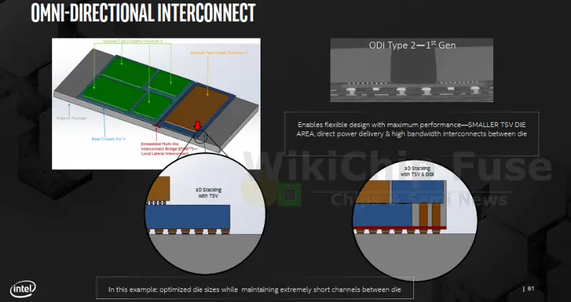
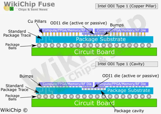
ODI currently comes in four variants. In calls the two major options ‘Type 1’ and ‘Type 2’. There are two flavors of each type – a copper pillar vs cavity. All four variants may be combined together as needed. Likewise, bottom ODI dies may be active dies, passive dies, or a combination of both.
| Type 1 | Type 2 |
|---|---|
| Bottom die between the top die(s) | Bottom die(s) are completely under a top die |
Type 1: Between Two Top Dies
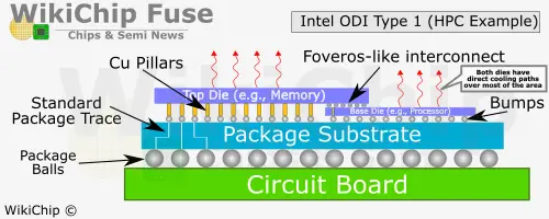
In ODI Type 1 the die is placed below two top dies or alternatively, below a single die that doesn’t entirely cover the bottom die. In ODI1 the bottom die covers only the portion of the top die where bonding is required, inheriting the Foveros-like interconnect advantages while eliminating the TSV disadvantages. ODI1 can be passive as in the case of something as simple simple routing from die-to-die or active as in the case of actively routing data among multiple dies or providing highly localized cache directly under multiple dies. It’s also possible to use this type with a single die such as in the case of a processor with HBM or some other logic.
For high-performance applications where heat is an even more of a concern, ODI1 provides the added advantage found in standard 2.5D interposers which is direct access to cooling solution without obstructions. One example Intel provided is one involving a microprocessor with direct connection to stacked memory. ODI avoids the complete stacking of the two dies thereby providing both dies with direct cooling solution access. At the same time, this version retains the high-bandwidth Foveros-like interconnect between dies while removing the need for long a channel that goes through a silicon interposer.
On its surface, the Type 1 Cavity version may seem very similar to a standard EMIB, however, it is quite different. The ODI die in this version is not actually embedded in the silicon with routing capabilities surrounding it on all sides. The base ODI die is placed inside the cavity at a controlled height using thermal compression bonding. TCB is then used to attach the top die. By controlling the height of the bottom die independently, they are able to maximize the C4 process.
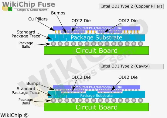
Type 2: Entirely Under Top Dies
In the ODI Type 2, the die is completely under a top die. In this situation the bottom die can be positioned exactly where it is needed closest in terms of routing path to the desired logic in the top die, much in the same way as you would with land-side capacitors (LSC) to maximize their efficiency. ODI2 may be used to enhance the benefits of a top die such as by attaching additional I/O capabilities or localized cache. Alternatively, it can be used to add another layer of major functionality such as by attaching an accelerator directly beneath a processor.
Mix and Match
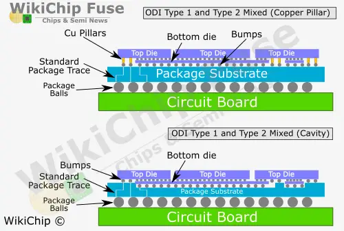
One of the interesting features of ODI is that all the various options may be mixed and matched as desired and where it makes sense. For example it’s possible to make the base die much larger to encompass multiple top dies in a Type 2 configuration but have the edge dies be in a Type 1 configuration, allowing their power delivery to escape through copper pillars instead.
Intel has been rolling out an impressive number of new packaging technologies covering an array of capabilities and functionalities. It has taken a number of years since their first disclosure of EMIB until production of chips such as Kaby Lake G started rolling out of the line. Given Intel’s initial disclosure of ODI in late 2019, we probably won’t see this technology for another number of years – likely in the 2022/23 timeframe, however as EMIB and Foveros technologies mature, it’s likely that we will see further integration of new capabilities, beyond ODI, accelerating into production at a faster pace.
–
Spotted an error? Help us fix it! Simply select the problematic text and press Ctrl+Enter to notify us.
–