
TSMC Talks 7nm, 5nm, Yield, And Next-Gen 5G And HPC Packaging
Next-Generation Packaging
The need for chiplet-based solutions continues to grow as leading-edge nodes increase in complexity and cost. The three main reasons is splitting up dies into smaller chiplets for yield and binning purposes, leveraging older, mature, nodes for analog and other parts of the SoC that does not necessarily scale well, and higher system integration through components such as HBM.
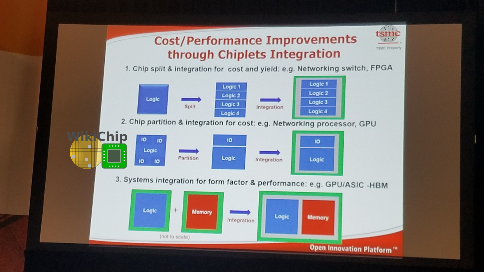
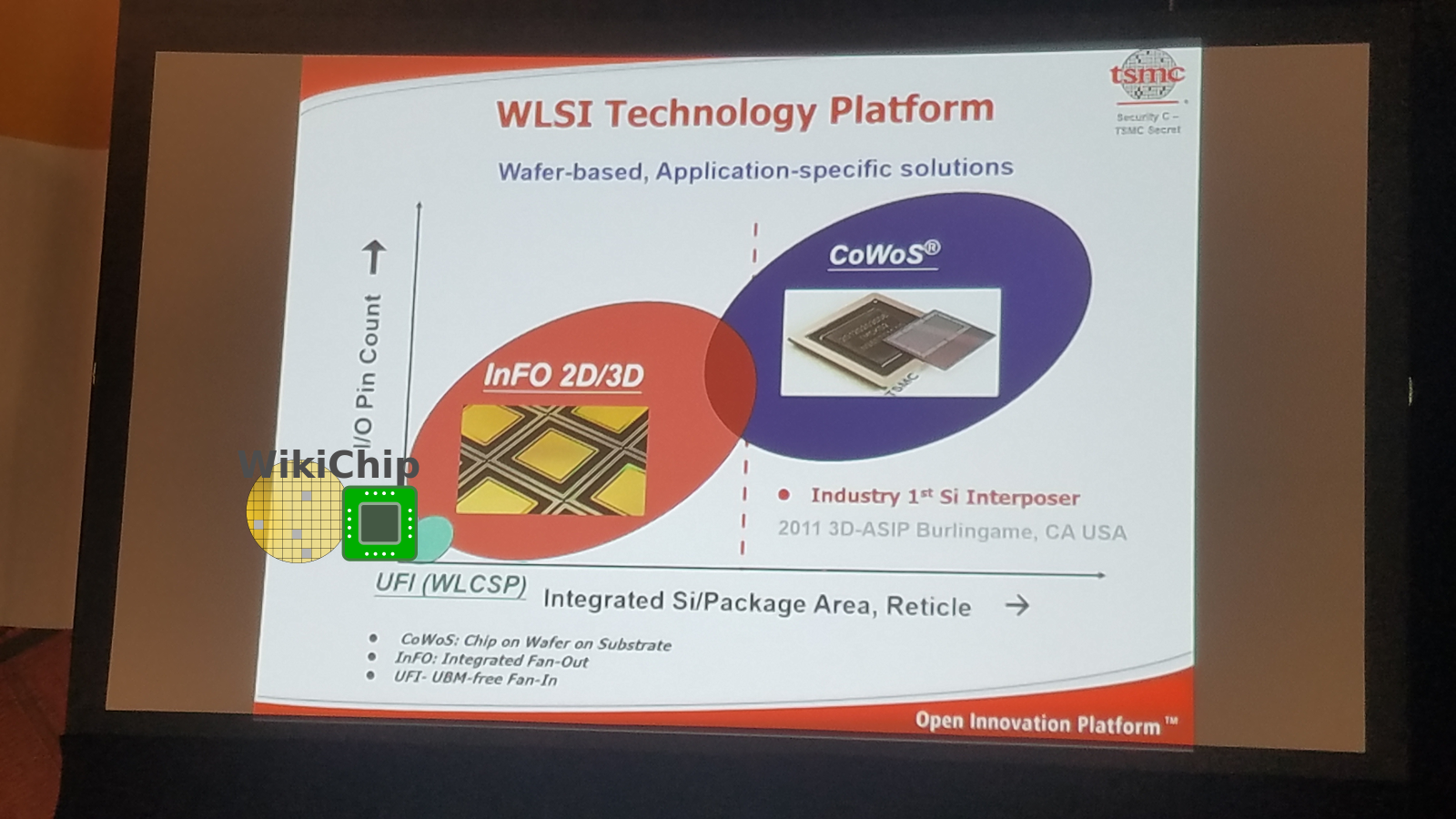
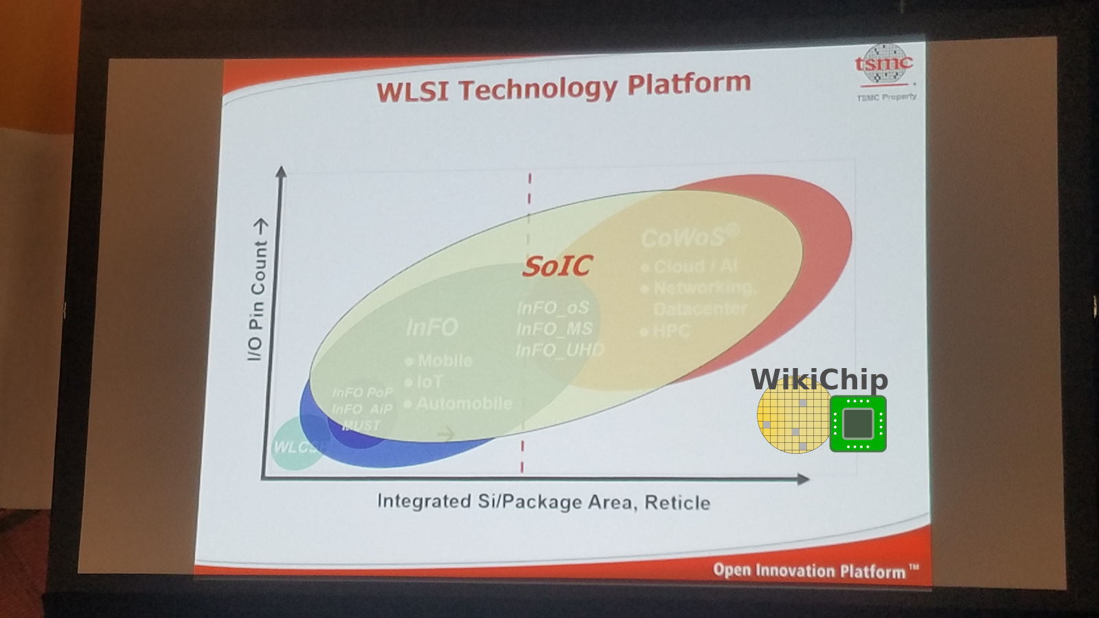
TSMC offers numerous technologies as part of its wafer-level system integration (WLSI) platform which is designed to cover everything from low-idle mobile applications all the way to high-performance computing. Their chip-on-wafer-on-substrate (CoWoS) packages targets AI, networking, and HPC applications while their integrated fan-out (InFo) packaging targets networking and mobile applications.
TSMC InFO packaging is their general fan-out wafer-level packaging (FOWLP) solution which comes in many different flavors depending on the application. InFO uses dense RDL and fine pitch through package vias (which TSMC also calls through-InFO vias or TIVs). Their integrated fan-out on substrate (InFO_oS), InFO with memory on substrate (InFO_MS), and InFO ultra-high-density (InFO_UHD) are for anything from high-performance mobile to networking and HPC applications.
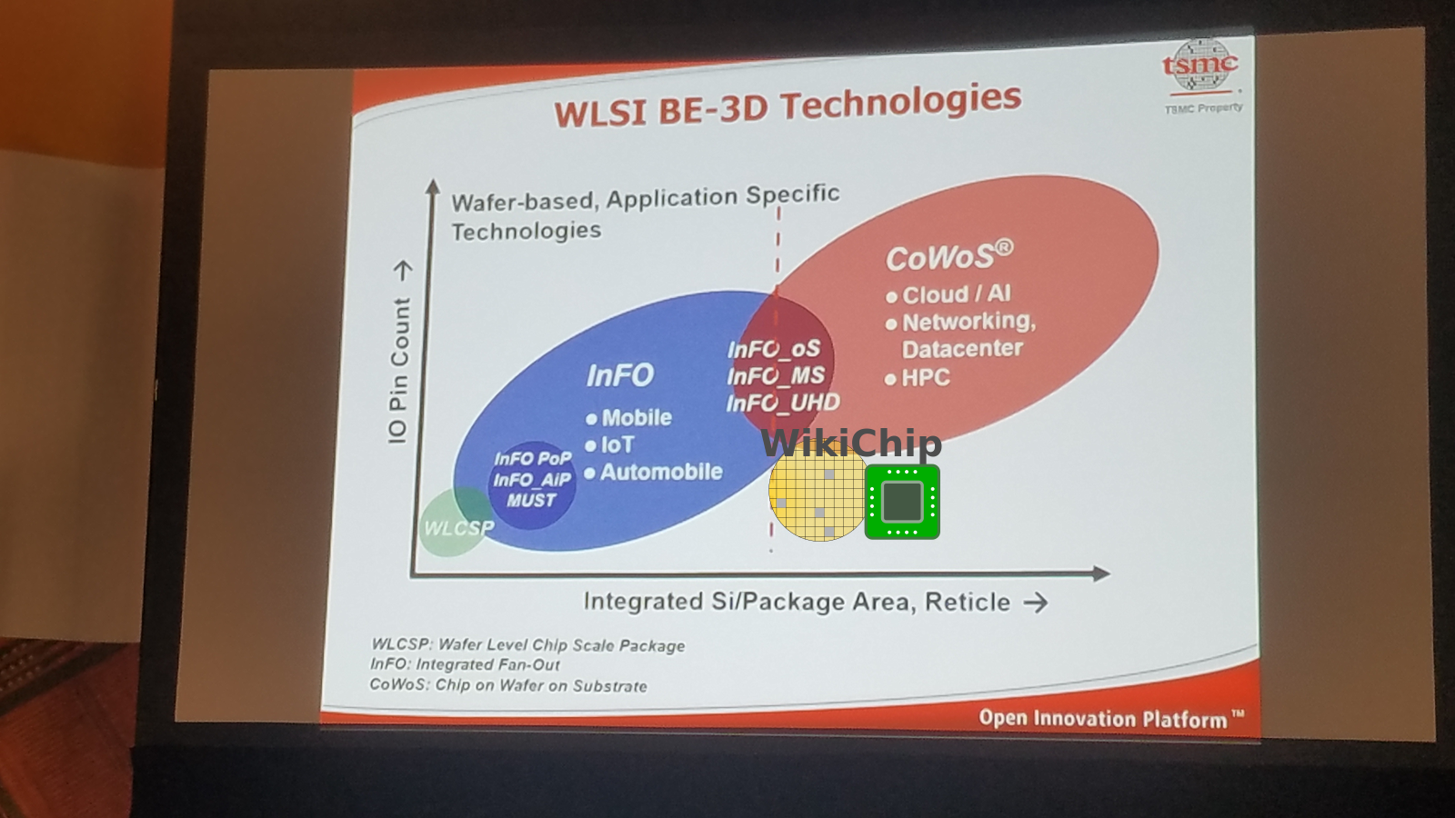
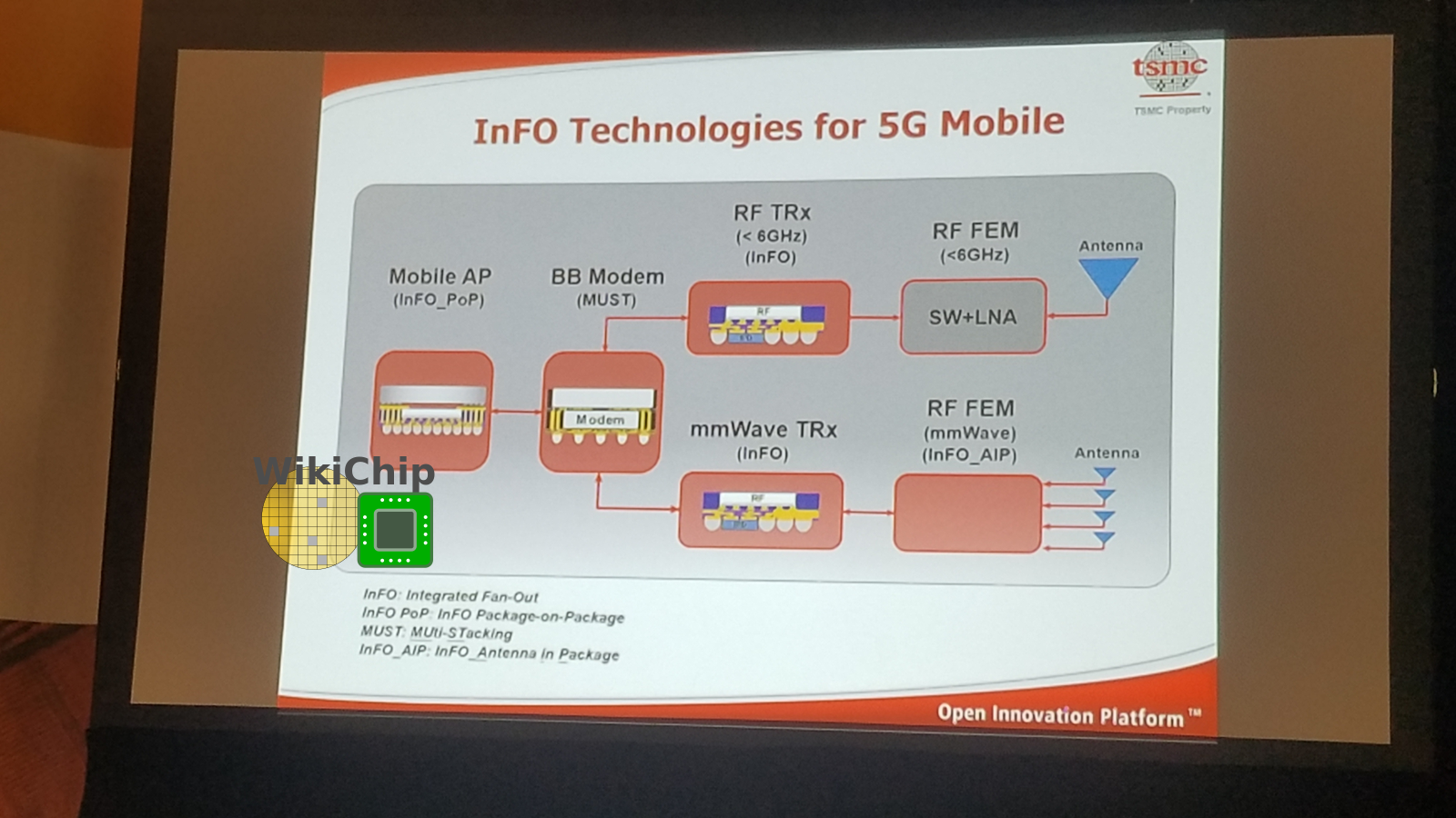
Specifically for the 5G mobile platform, TSMC has InFO POP (InFO_POP) for things such as mobile AP applications, InFO Antenna-in-package (InFO_AiP) for RF front-end module (FEM) applications, and Multi-stack (MUST) for baseband modems.
3D-MiM For Higher Bandwidth
One of the earliest examples of InFO_POP was the Apple A10 (prior processors featured conventional POP) which was released in 2016. However, even InFO_POP has the shortcomings of being memory bandwidth limited due to the controller and TIV pitch. This problem is further aggravated with upcoming 5G and AI edge/mobile applications that are inherently more memory bandwidth bound. Trying to overcome this problem, TSMC announced the 3D-MUST-in-MUST packaging technology (note that MUST stands for multi-stacking). 3D-MiM integrates multiple vertically-stacked memory chips through integrated fan-out (InFO) WLS integration using high-density RDL and fine pitch TIVs. As you might imagine, the I/O must be exposed on just one side of the chips which are independently connected to the SoC, forming a wide I/O interface.
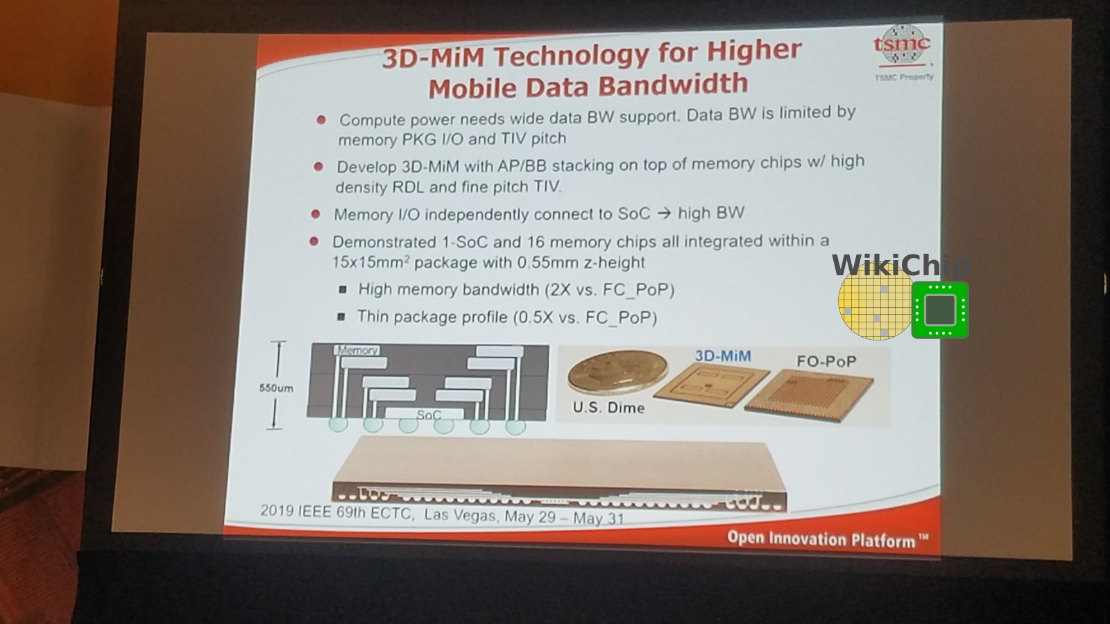
TSMC demonstrated the technology on an SoC with 16 memory chips in a single package. The chip had a footprint of 15 mm by 15 mm with a z-height of just 0.55 mm. Compared to a flip-chip POP package, that chip has twice the memory bandwidth at half the height.
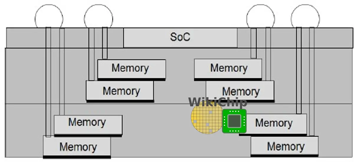
TSMC touted a number of other advantages. Since there is no substrate and no bumps, the distance from the memory I/O to the SoC is much shorter, yielding better electrical performance characteristics. Additionally, the thinner profile is said to deliver better thermal performance.
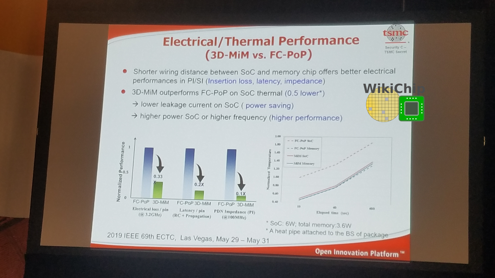
By the way, 3D-MiM is not limited to a single SoC. Actually TSMC talked about using multiple SoCs along with very large number of memory chips (e.g., 2 SoCs with 32 memory chips) in order to create HPC applications with high bandwidth and lower power as an alternative technology to current 2.5D such as HBM. A key difference here is that the InFO memory chips are each individually directly connected to the SoC without the need for a base logic die.
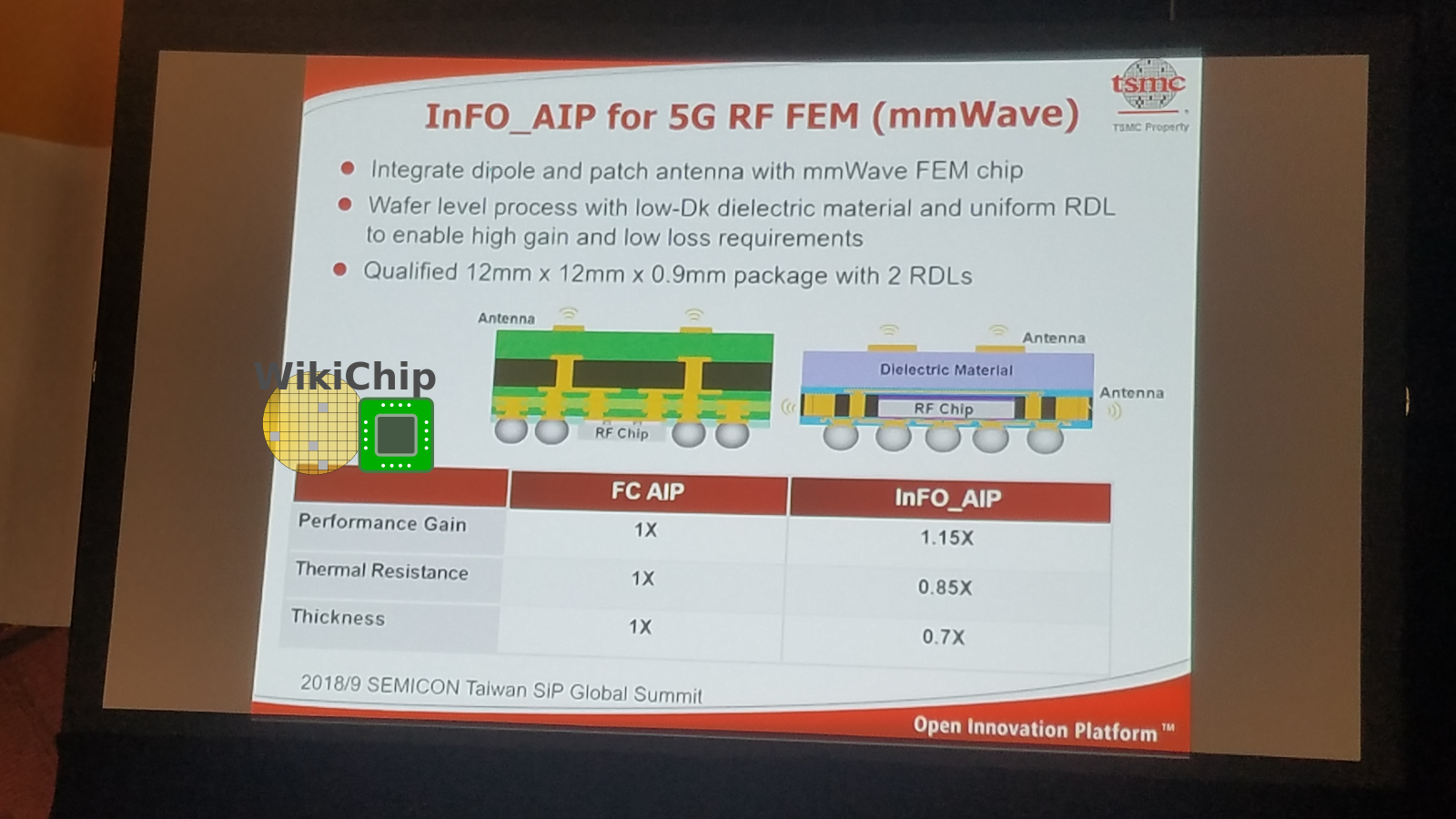
InFO Antenna-in-Package (InFO_AiP)
Targeting specifically 5G millimeter wave system integration, TSMC developed the InFO antenna-in-package (InFO_AiP). What this package attempts to address is the link – or interconnect – between the actual chip and the antenna which can suffer significant transmission loss. TSMC does this through a slot-coupled patch implemented in the RDL along with an embedded RF chip in the molding compound itself which is directly interconnected to the RDL without bumps.
Since the performance of the interconnects between the antenna and the chip is a function of the roughness of the surface and the transition between the chip and the package, InFO material and RDL uniformity allows for much lower transmission loss. Compared to flip-chip AiP, TSMC claims it can provide up to 15% higher performance, has 15% lower thermal resistance while having a 30% lower profile.
Networking And HPC
For high-performance computing and networking applications, TSMC offers CoWoS and InFO on substrate and with memory (_oS/_MS).
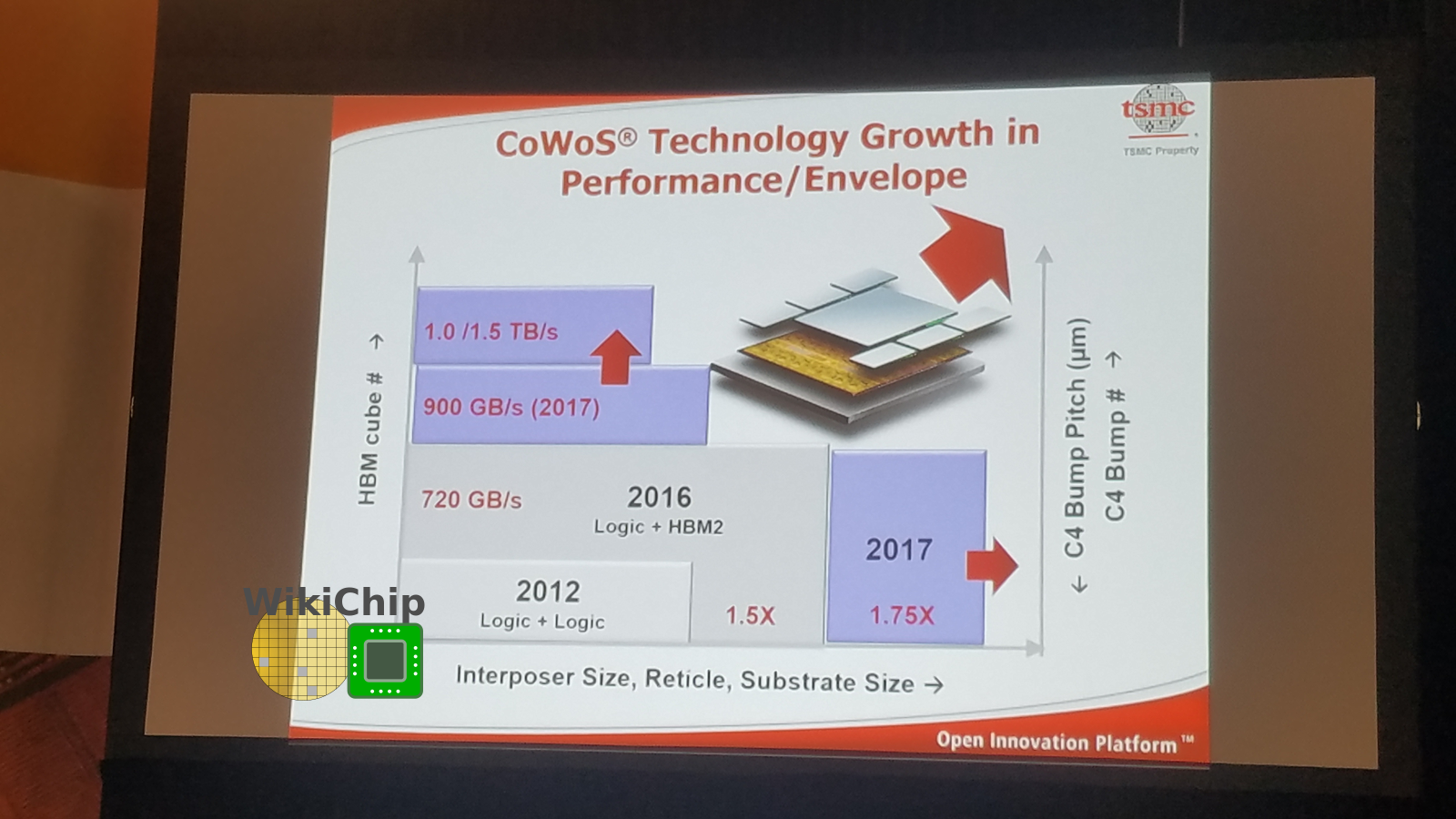
CoWoS can extend to 2 reticles with aggressive line/spaces of 0.4 μm / 0.4 μm. This is a very mature technology with very high yield which has been in volume production for over five years. CoWoS has been used extensively for GPUs but can also be found in various networking applications. TSMC says they have had over 15 tapeouts so far.
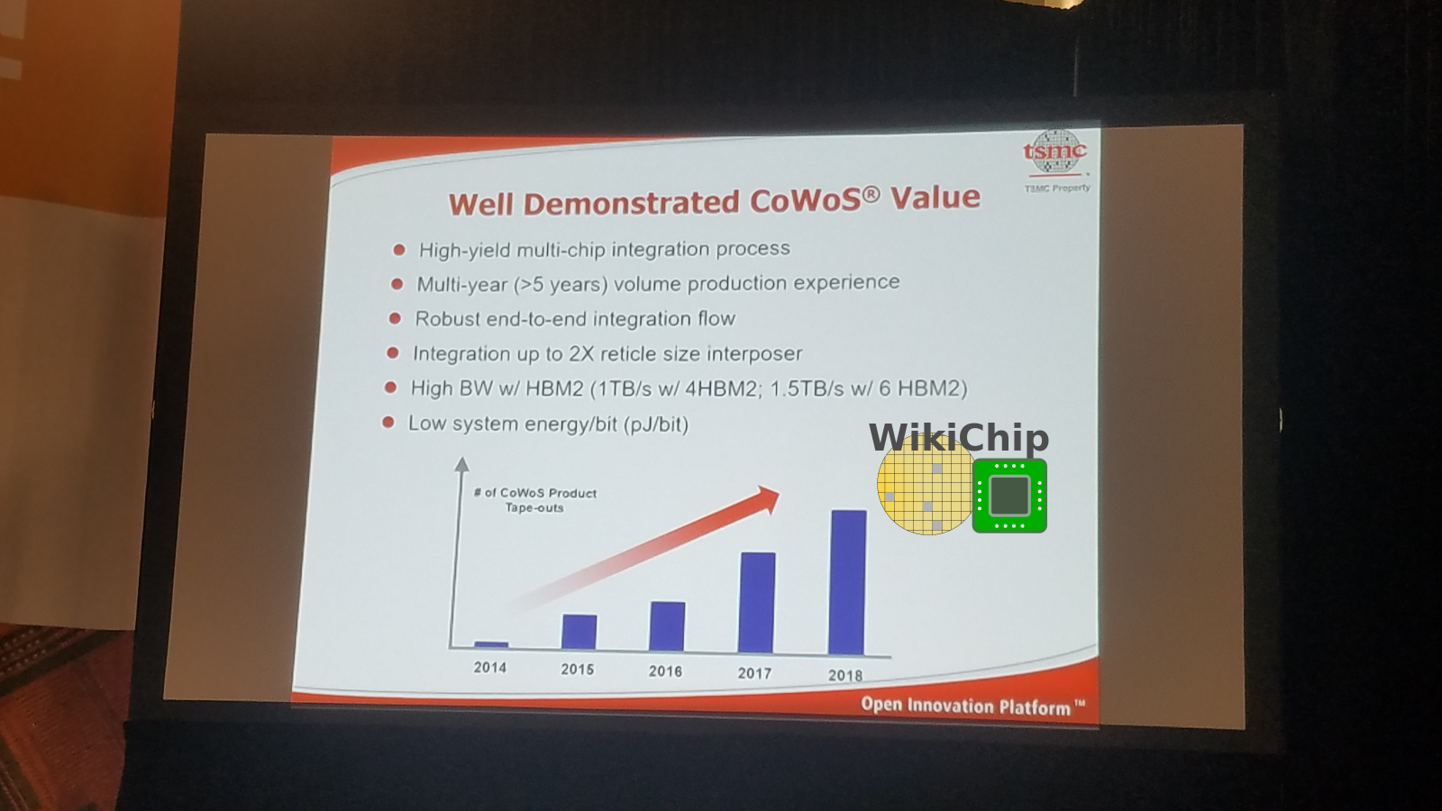
Currently, CoWoS supports up to 1.5 TB/s with 6 HBM2 blocks. TSMC reports working on higher bandwidth solutions along with larger silicon areas beyond 3 reticles.
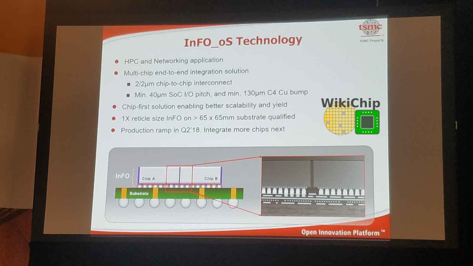
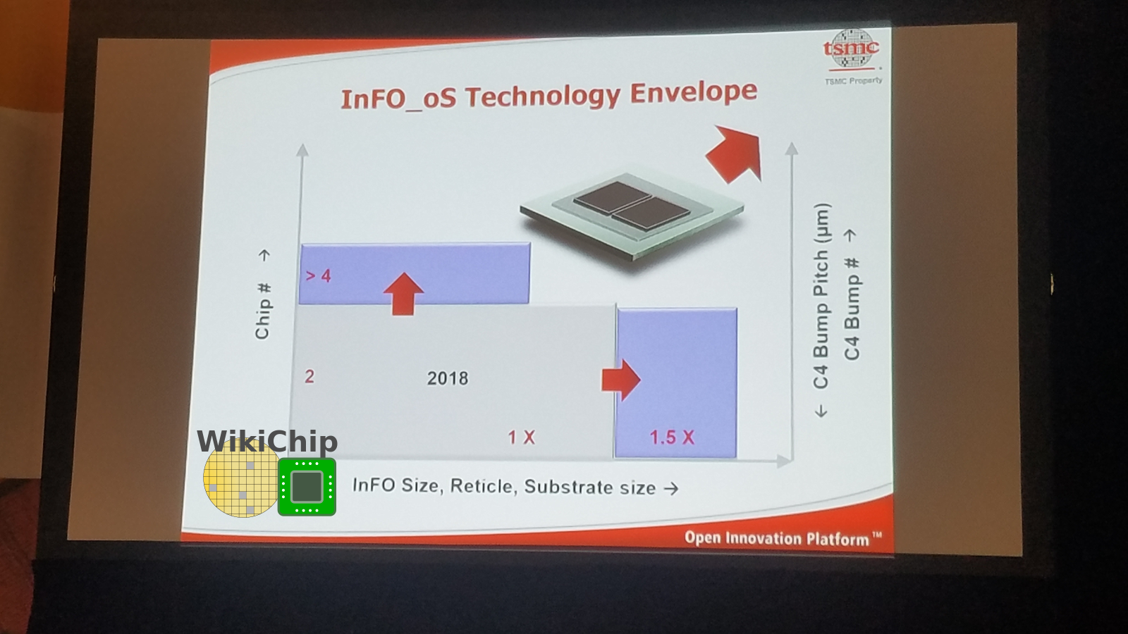
For networking applications, TSMC offers InFO on substrate which can reach integrated Si areas of up to 1 reticle but has a slightly more relaxed L/S pitch of 1.5 μm / 1.5 μm. Current technology features a minimum I/O pitch of 40 μm and a minimum C4 bump pitch of 130 μm. Production of InFO_oS ramped in the second quarter of 2018. They are currently working on enabling the integration of more than two chips and along with a silicon area of 1.5x reticle size.
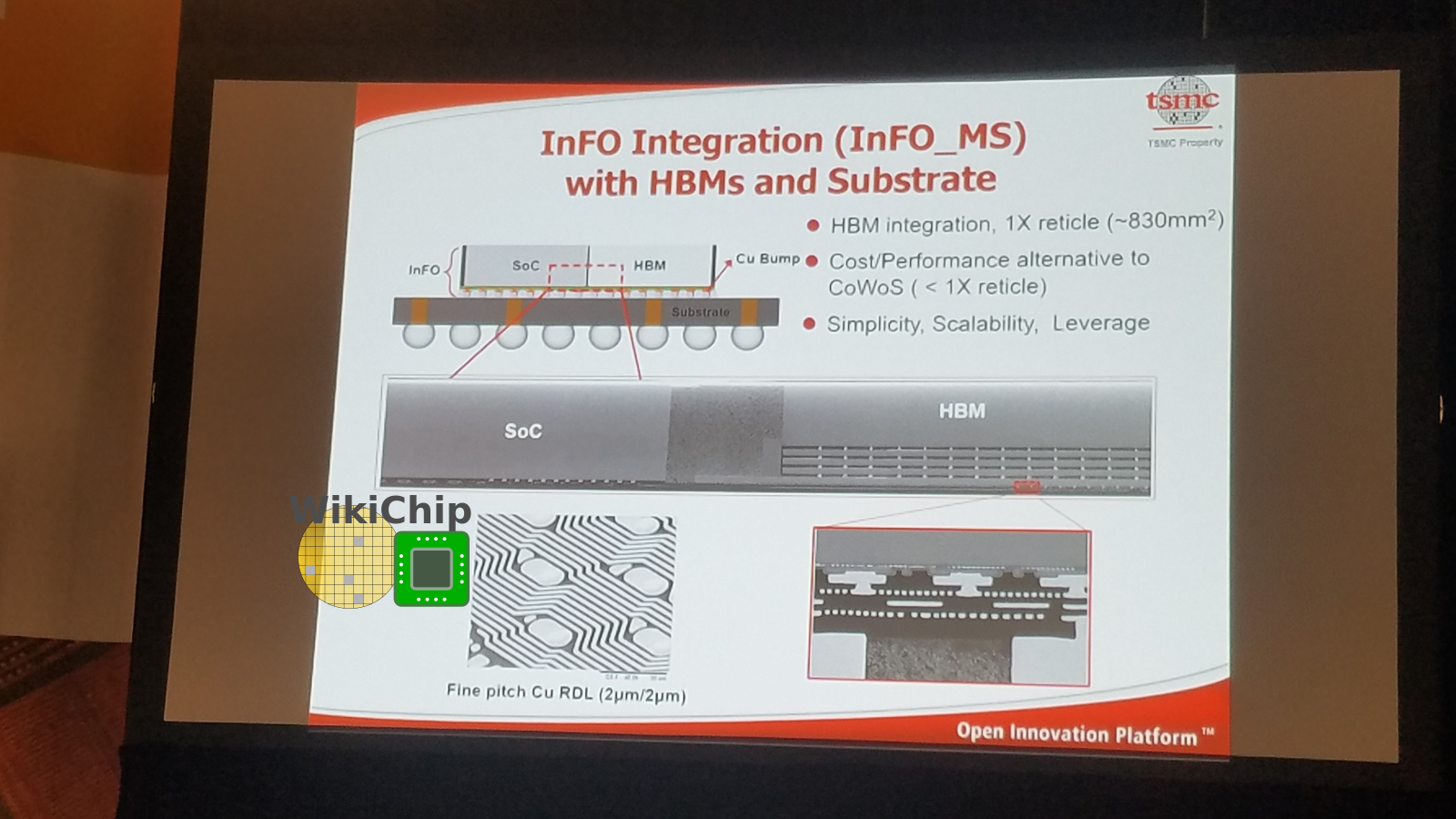
For AI applications and similar workloads, TSMC has InFO with memory on substrate designed to integrate with HBM. This technology currently features RDL L/S of 2 μm /2 μm and is limited to a single reticle. In many ways TSMC is billing InFO_MS a performance-cost sensitive alternative to CoWoS.
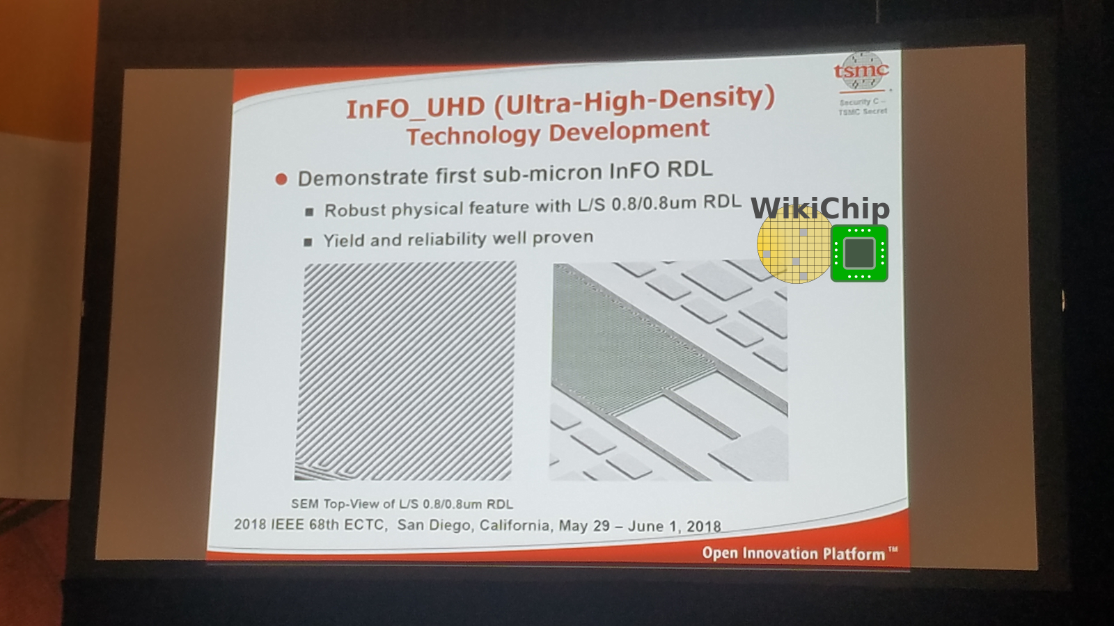
InFO Ultra-High Density (InFO_UHD)
The two key parameters that drive performance and power is the writing density and bump pitch. That’s the goal behind the InFO Ultra-High Density packaging which TSMC has reported achieving 0.8/0.8 μm L/S for 500 wires/mm and features up to 10000 bonds/mm².
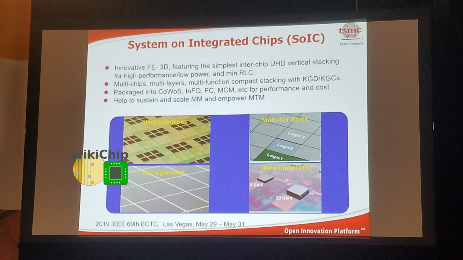
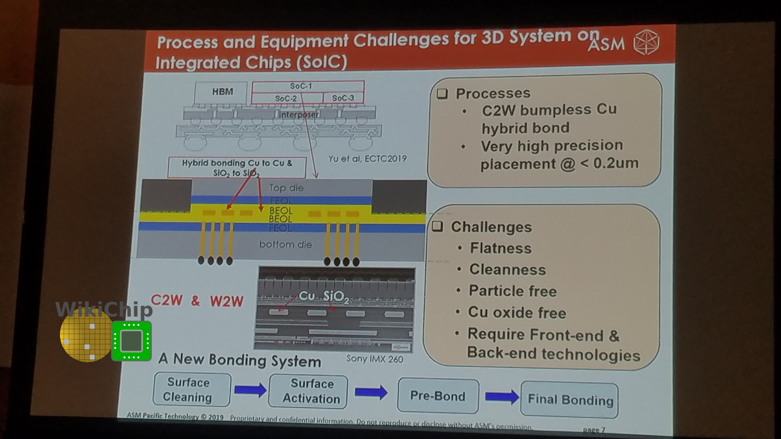
System-on-Integrated-Chips (SoIC)
Everything described above leads to SoIC. SoIC is their next-generation “true” 3D packaging technology. SoIC is a chip-on-wafer (CoW) stacking approach that allows mix-and-match integration of many different KGDs or even stacks of KGDs to be integrated together – varying in sizes and process nodes. It is both a face-to-face and face-to-back technology. Because from the outside, it looks like any other standard chip, you can actually combine an SoIC with existing technologies such as InFO, CoWoS, or flip-chip in the same package. Like the InFO_UHD, it currently features 10000 bonds/mm² and they believe they can eventually reach 1 million bonds/mm² with the introduction of “SoIC+”.
–
Spotted an error? Help us fix it! Simply select the problematic text and press Ctrl+Enter to notify us.
–