
Radeon RX 5700: Navi and the RDNA Architecture
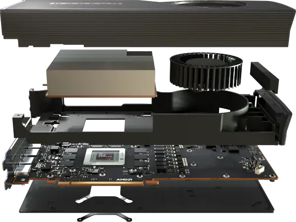
Last year AMD launched the Radeon RX 5700 Series. This GPU is part of AMD’s latest Navi microarchitecture which makes use of the new RDNA architecture. At ISSCC AMD gave a short talk about the 5700 and some of its design points. The speaker was Sal Dasgupta, director at AMD also serving as the lead the power and performance team on the RX 5700 project.
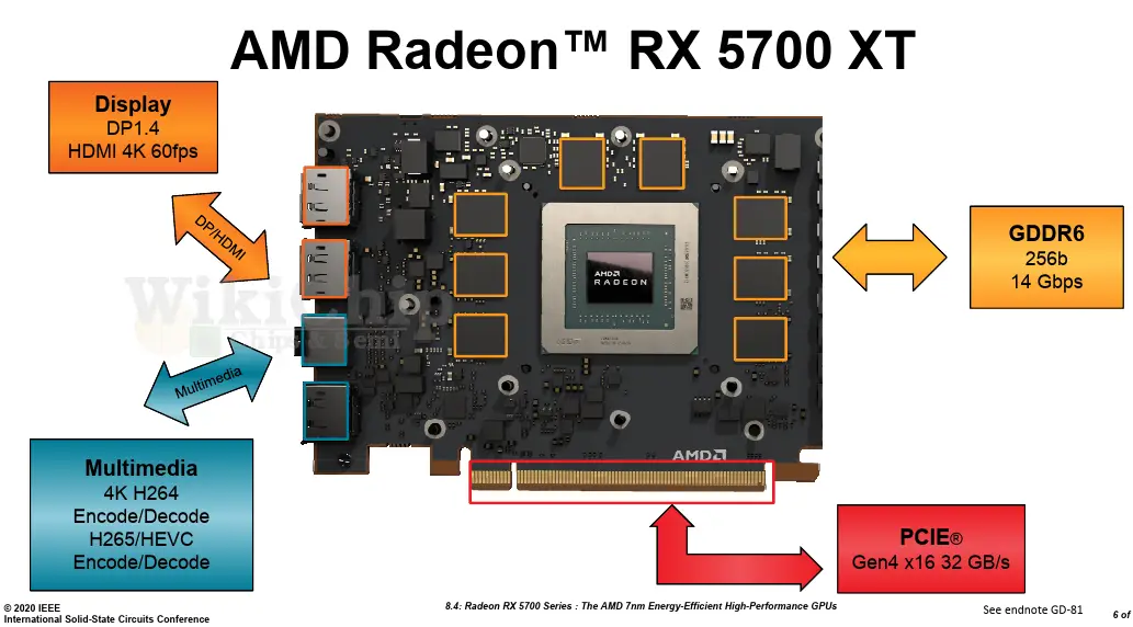
The reference board for the Radeon RX 5700 XT is shown in the slide below. As far as display is concerned, there is support for DisplayPort 1.4 and HDMI 2.0 which supports 4K at 60 fps and 1080p at 240. From a multimedia point of view, there is decode and encode support for H264 and H265. Although this isn’t in the slide, there is also VP9 decode support. The board interfaces with the system over sixteen lanes of PCIe Gen4. Finally, for the DRAM interface, the chip supports a 256-bit GDDR6 interface operating at 14 GT/s.
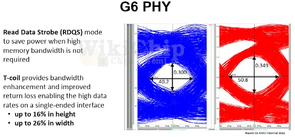
The 5700 uses GDDR6 memory. AMD has gone back and forth between HBM and GDDR a couple of times. Compared to GDDR5, GDDR6 operates at nearly double the data rate (14 GT/s vs 8). With an interface 256-bit wide, you are looking at a peak bandwidth of 448 GB/s which is 75% higher than the RX 580 but 8% lower than the Vega 64. Sal explained that the switch back from HBM2 to GDDR6 was really due to the platform cost. Given all the changes that were made and taking into account the platform power (incl. GDDR6 memory) and the bandwidth provided, it was determined that this was suitable enough for their target performance at the target cost. It goes without saying that future models might go a different route.
In addition to the interface itself, there are a couple of new power-related features that come with this move. Read Data Strobe (RDQS) support saves power when in idle power states. Moving from 8 GT/s to 14 GT/s was helped by a T-coil which helped improve the eye height by up to 16% and eye width by up 26%.
AMD reported significant improvements compared to the prior generation. AMD says it was able to increase the maximum turbo frequency by 23% while increasing the IPC by 25% while, at the same time, lowering the power consumption by 23% which in total equates to around 1.5x greater performance per watt. Some of those improvements come from the new process technology, some of it comes from better physical design, and some of it is architectural.
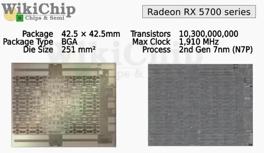
Some of the die and package specs are listed below. The new chip comprises 10.3 billion transistors on a 251 squared millimeter piece of silicon. One important key feature to point out is the underlying process technology which is TSMC’s 2nd-generation 7-nanometer node (N7P) which not only provides significant density improvement over AMD’s last node, GlobalFoundries 14-nanometer process but also offers slightly better performance and power over the company’s own first-generation 7 nm process.
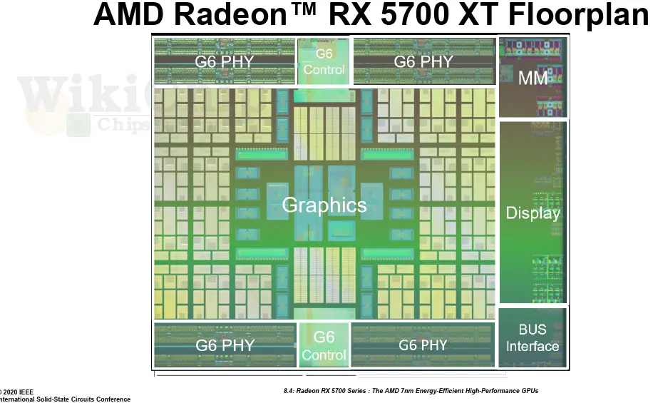
At the center of the die is the graphics core. The entire north and south sides are the GDDR6 controllers and PHYs. On the east side of the die are multimedia, display, and bus interfaces. Dasgupta didn’t want to spend too much time on the floorplan which he said involved quite a bit of careful layout as AMD has additional papers on this coming up in future conferences. We’ll have to wait for those delighted papers for more details!
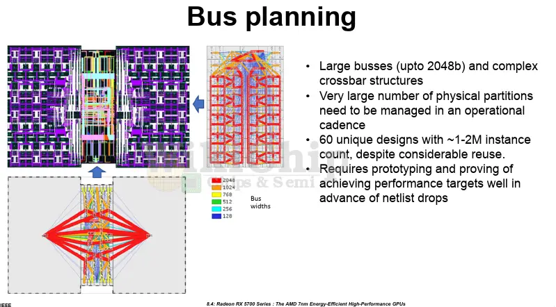
AMD made a lot of work on the physical design side. With over ten billion transistors on the chip and with highly parallel architecture, the large wire count alone poses new challenges on the power delivery. The 5700 includes buses that are up to 2048-bit wide. Although there has been a lot of physical reuse, there were still around 60 unique tile designs, each with one to two million instance-counts. Physical design played a big role in the careful placement of logic to alleviate routing issues. The 5700 is implemented using 13 metal layers. Custom routing in the upper low resistance wires is taken advantage of on critical paths to minimize wire delays and improve timing across. It’s a nice reminder that adding more compute units isn’t as simple as just finding a spot for them, there are rather complex physical routing issues involved as well.
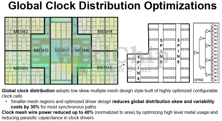
The large graphics core mesh actually comprises seven smaller meshes in order to better handle the clock distribution while keeping the overhead at a minimum. AMD claims that the move resulted in a reduction of global clock skew by 30%. Another optimization that was done is introducing custom-designed clock buffers. Reducing parasitic capacitance in the drivers along with metal wire optimizations contributed to another 40% reduction in the power contribution of the clock mesh, normalized by area.
Within the local clock distribution, AMD adopted a configurable structured clock tree. The structured clock tree allowed them to reduce the median clock insertion delay by up to 50%, reducing jitter and variability. For those local clock trees, AMD went with a more bottom-up approach instead of a fixed-region cloning style methodology. The change allowed them to reduce the effective switched capacitance by up to 10% iso-process.
Short Comparison
The RX 5700 XT is the first generation to implement the RDNA architecture. Compared to the prior generations which supported GDDR5 and then HBM2, this chip switches back to GDDR6. The 5700 is manufactured on TSMC 7-nanometer process while the other two were based on GlobalFoundries 14-nanometer process. The other main points in the table are the boost clock and the board power which decreased while the clock improved. AMD says that when normalizing for iso-power and iso-configuration, the 5700 brings around 50% higher performance.
We want to bring your attention to the bottom right side of the slide below which reports on the contributors of this performance uplift. One of the major contributors to this 50% improvement in performance is the move to a 7-nanometer node which accounts for 30% of this alone. On top of that, the density advantage enables the remaining changes. It’s a nice reminder that despite what you might have been led to believe, the effects of transistor scaling and Moore’s Law remains the driving force behind new products. The remaining contributors are the higher clock and power improvement (10%) and the remaining 60% of that came from the performance per clock improvement as a result of the RDNA architecture.

–
Spotted an error? Help us fix it! Simply select the problematic text and press Ctrl+Enter to notify us.
–