
Radeon RX 5700: Navi and the RDNA Architecture
RDNA
The 5700 integrates 40 RDNA compute units, a multi-level cache comprising an L2, L1, and L0, a geometry engine, 64 pixel units, and 4 asynchronous compute engines. One of the main design goals that AMD doubled down on was higher frequencies at lower power across all those components.
Inside the graphics core of the die, in the center is the command processor which interfaces with the software over the PCI Express interface. Next to the command processor is the geometry processor which assembles the primitives and vertices. It is also responsible for distributing the work among the two shader engines. The two shader engines house all the programmable compute logic. Within each shader engine, there are two shader arrays. Inside each array is the primitive unit, a rasterizer, a group of four render backends (RBs), a shared L1 cache, and the new compute units.
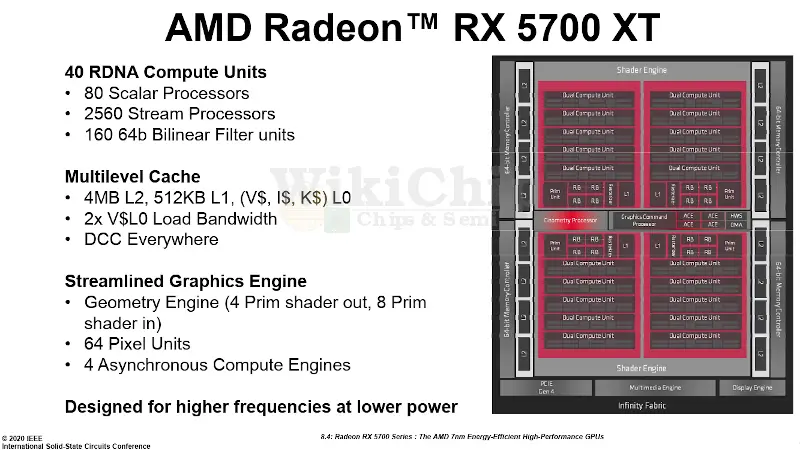
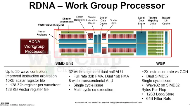
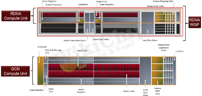
The big differences with RDNA show up in the compute units of the shader array. Inside each of the shader arrays are five RDNA work group processors (WGPs). The RDNA WGP incorporates two RDNA compute units compared to one GCN compute unit in the prior architecture. It’s worth pointing out that since there are two compute units within a WGP, the local data share (LDS) is shared between the two. Additionally, in the GCN CU AMD had four SIMD16s whereas, in the new RDNA CUs, there are now two SIMD32s. Another difference is that the texture cache in the GCN compute unit is a level 1 cache whereas the cache in the RDNA CU is a level 0 cache.
If you were to do some back-of-the-envelope calculation, building the 5700 back from the WGPs, with two shader engines you are looking at twenty work group processors which translates to eighty scalar processors. With each being SIMD32, that gives us a total of 2,560 stream processors. On Navi, they operate at full rate 32b FMAs (or dual 16b FMAs). With a peak frequency of 1,910 MHz, you are looking at a peak compute of 9.779 teraFLOPS (SP) and 19.56 teraFLOPS (HP).
The major reason for the SIMD organizational changes is the utilization of hardware. The RDNA (and GCN) operate on kernels comprising instruction streams that usually operate on large amounts of data in parallel called work-items. Work-items are further packaged into work-groups that inter-communicate through the LDS. Stepping a bit further, those work-groups are subdivided by the shader compiler into wavefronts. Wavefronts are the important unit here as it’s the microarchitectural grouping of work-groups (and hence work-items).
In the prior GCN architecture, wavefronts contained 64 work-items. When all work-items executing the same instruction, this works fantastically well and with SIMD16, you get very good efficiency over the four cycles that require to do the entire wavefront. However, the disadvantage comes when you consider newer workloads that feature more complex control flow. When that happens, the wavefront no longer features a homogeneous operation. This results in lower utilization of the underlying hardware resources. RDNA promises to alleviate this problem by narrowing the size of the wavefront to 32 work-items (appropriately named Wave32). And as we noted earlier, Navi is configured as SIMD32, twice as wide as the vector ALUs in Vega, matching the size of the native wavefront. This should enable Wave32 to do work every cycle and better utilize the available resources more. Additionally, the narrower wavefronts should, at least in theory, make more complex control flow divergences cheaper.
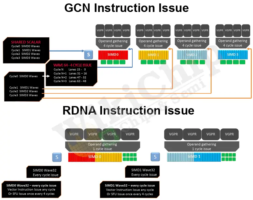
By the way, beyond the potential utilization and performance premise, there are other more subtle advantages on the implementation side. With the vector instructions issuing every cycle, you get the opportunity to potentially get rid of some buffers required to store intermediate signals and values, reducing data movement and wasted energy. It should also simplify the control logic involved for execution.
The cache subsystem was also redesigned. In Navi, a new L1 unit has been added between the compute units and the L2. What was previously L1 is now called an L0. The L1 is actually a read-mostly memory. Any writes to the L1 actually invalidates the cache lines in the L1 and writes to the L2. For that reason, writes usually bypass the L1 to the L2 directly. The L1 is shared by the entire shader array across multiple work group processors. It also services requests from the pixel units within the array. The new additional layer of the cache was added in order to reduce the latency and improve the bandwidth. Previously, the L2 served all misses from the L1 within the compute units. On Navi, much of that role was moved to the L1 which centralized the entire shader array caching operations. The 7nm process punishes sending data over long wires and there is a growing need to reduce that. The L1 cache also reduces the congestion on the L2 and simplifies its overall design, but it’s really there to fight the parasitics brought about by 7-nanometer wires.

Power
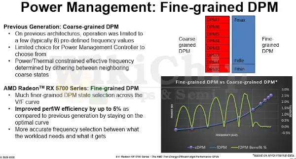
The RX 5700 features fairly complex power management designed to manage the classic clock and voltage and maximize performance during active workloads while minimizing power during less active workloads and idle time. Navi adds a couple of new power management features to address some of the previous shortcomings. AMD reported on two new power management features that were added in this generation: per-part Fmax and fine-grained DPM.
In the prior generation, there were eight discrete DVF states. The effective frequency of the chip ultimately had to snap into one of those slots. With Navi, AMD moved to a fine-grained DPM which more closely followed the natural voltage-frequency curve of the chip. If this feature sounds familiar to you, it’s because the technology was in fact borrowed from the CPU designers. On the Zen architecture, AMD calls it Precision Boost 2 technology and it gets rid of the quantized V-F states. AMD claims that the switch has allowed them to improve the performance/W efficiency by up to five percent.
In the prior generation, the max frequency of any part is determined by the slowest part in the distribution. In other words, understandably, the faster parts are artificially limited by the slowest parts. Those DVFS settings were set by the heuristics of a high-power workload. With Navi, AMD added a per-part Fmax management which allows each part to run at its maximum frequency allowed at Vmax, removing the dependency on slower parts. For example, given two different workloads/applications with two very different power characteristics, you could potentially exploit that to run at two very different frequencies. Alternatively, at any given frequency, those two workloads will be operating at two very different powers. Ether way, the hardware has a little bit more room to play with, allowing parts to run at the Vmax of the platform or some other thermal constraint. The benefits are actually quite sizable. AMD claims that the decoupling of Fmax per part allows most parts to run at up to 15% higher Fmax on certain workloads.

–
Spotted an error? Help us fix it! Simply select the problematic text and press Ctrl+Enter to notify us.
–