
POWER9 Scales Up To 1.2 TB/s of I/O, Targets NVLink 3, OpenCAPI Memory for 2019
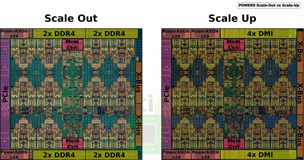
Last year IBM started rolling out their POWER9 processors. Those initial chips were based on their scale-out configuration. A month ago IBM launched the second part of their POWER9 rollout, the scale-up configuration. At Hot Chips 30, Jeff Stuecheli, IBM POWER architect, presented the POWER9 scale-up design and talked a little about what we can expect from POWER in the future.

Scale Up
Aimed at enterprise customers, POWER9 scale up differ from scale out in its I/O capabilities. In order to ensure a large design overlap between the two chips, both the scale-out and scale-up dies have identical silicon real-estate space – measuring 25.2 mm by 27.5 mm. The magic is in the PHYs.
Whereas the POWER9 scale-out processors use DDR4, scale-up leverages their custom memory-agnostic solution. The compact SerDes-based design leaves an additional Si area for more I/O. IBM uses that space to double the PowerAXON links. In addition to those changes, the scale up die also incorporates a third X-bus interface.
Memory-Agnostic I/F
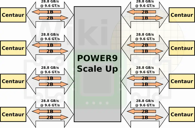
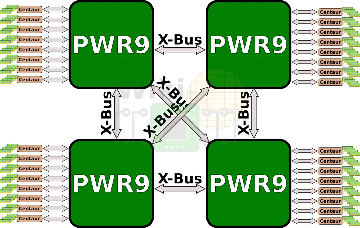
In POWER8, IBM introduced Centaur, a memory buffer chip. POWER9 continues to use Centaur. There are two memory controllers driving eight memory interfaces, each connected to a Centaur chip.
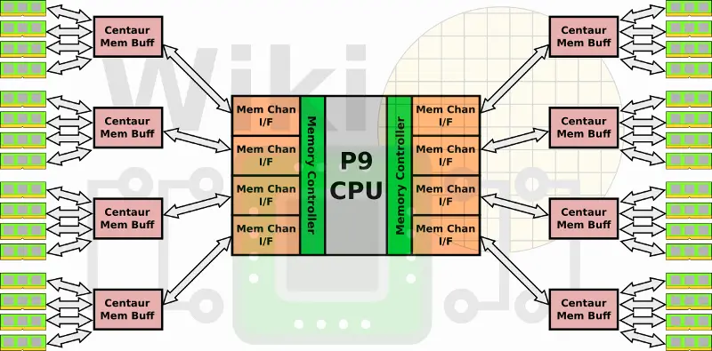
Each memory channel is capable of 1B write + 2B read at 9.6 GT/s or 28.8 GB/s for a total aggregated bandwidth of 230 GB/s across all eight channels. Since every Centaur chip has 16 MiB of L4 cache, there is a total of 128 MiB of L4 cache that can speed critical operations. By the way, the slide at Hot Chips showed each memory channel supporting 64 active operations, presumably 32 reads + 32 writes. This is identical to POWER8.
Stuecheli made sure to point out that since the memory interface talks in common commands, the DDR4 ports on the Centaur chip can be replaced by any one of the emerging memory technologies. Adding support for storage-class memories becomes a trivial change. For the time being, each Centaur chip has 4 DDR4 ports 10 bytes wide.
Multiprocessing
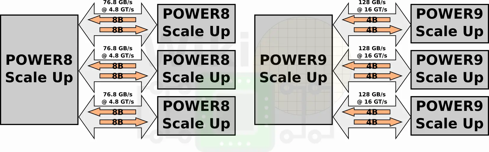
Communication between processors in the same drawer is done over IBM’s X-bus links. In POWER8 SU there were 3 links. Those were single-ended 4.8 GT/s links sending 8 bytes and receiving another 8. This provided an aggregated bandwidth of 230 GB/s. In POWER9 SU, the old interface was replaced with 16 GT/s differential signaling (sending 4 bytes and receiving 4). Despite half the width of the previous links, the 3.33x improvement in speed yields an aggregated bandwidth of 384 GB/s, a solid 1.66x improvement.
Compared to scale out, scale up has one additional X-bus link. With three links it’s possible to create a 4-way SMP with every processor connected to every other processor in a fully-connected topology. A 4-way SMP is the standard POWER9 drawer configuration.
PowerAXON
IBM introduced a new marketing term – PowerAXON – to group together their high-speed 25 GT/s interfaces. POWER9 scale-up has four 25G links.
One of the uses for those additional interconnects is IBM’s full 16-way configuration which makes use of 3 x24 lines. In this configuration, four IBM POWER9 SU drawers are linked together using their A-bus interconnects. In POWER8, there were 3 links operating at 6.4 GT/s (4B wide) for 25.6 GB/s per link and a total aggregated bandwidth of 76.8 GB/s. Since the new 25G links also double up as A-bus links, they operate at 25 GT/s resulting in over five times the bandwidth (400 GB/s).
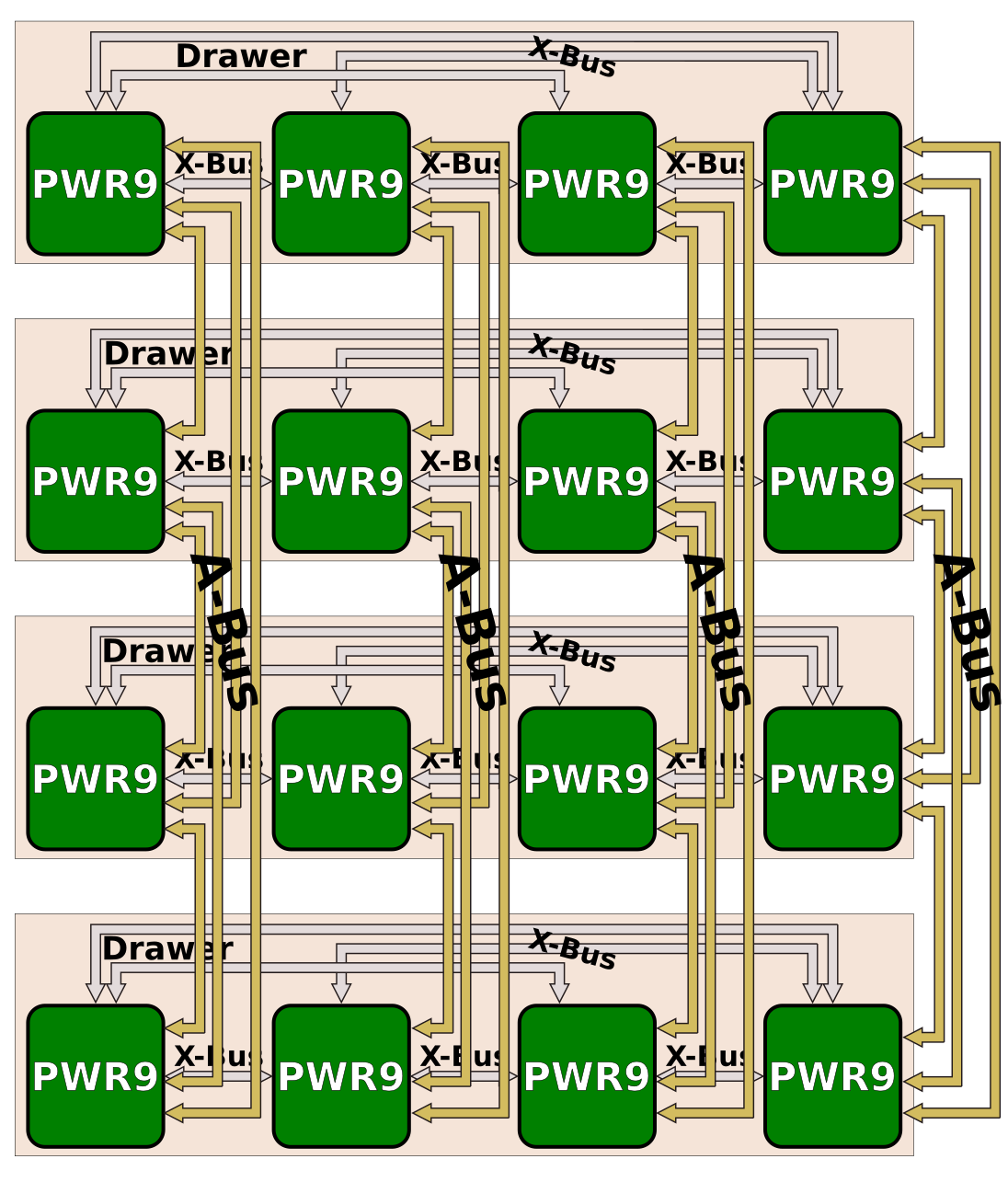
The 16-way is IBM’s usual two-hop configuration which only requires three A-buses. The remaining fourth link can be used for OpenCAPI or an NVLink GPU connection. Alternatively, by using the new A-Bus Link, POWER9 is now capable of providing an all-to-all fully-connected interconnected topology for their 8-way configuration.
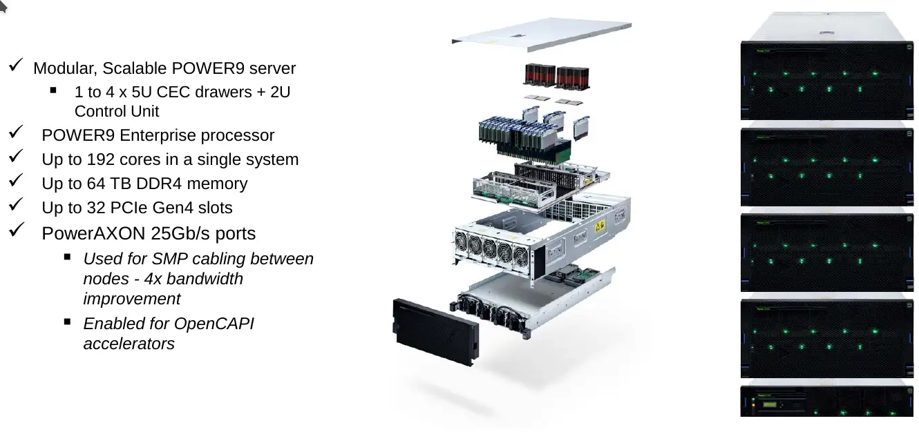
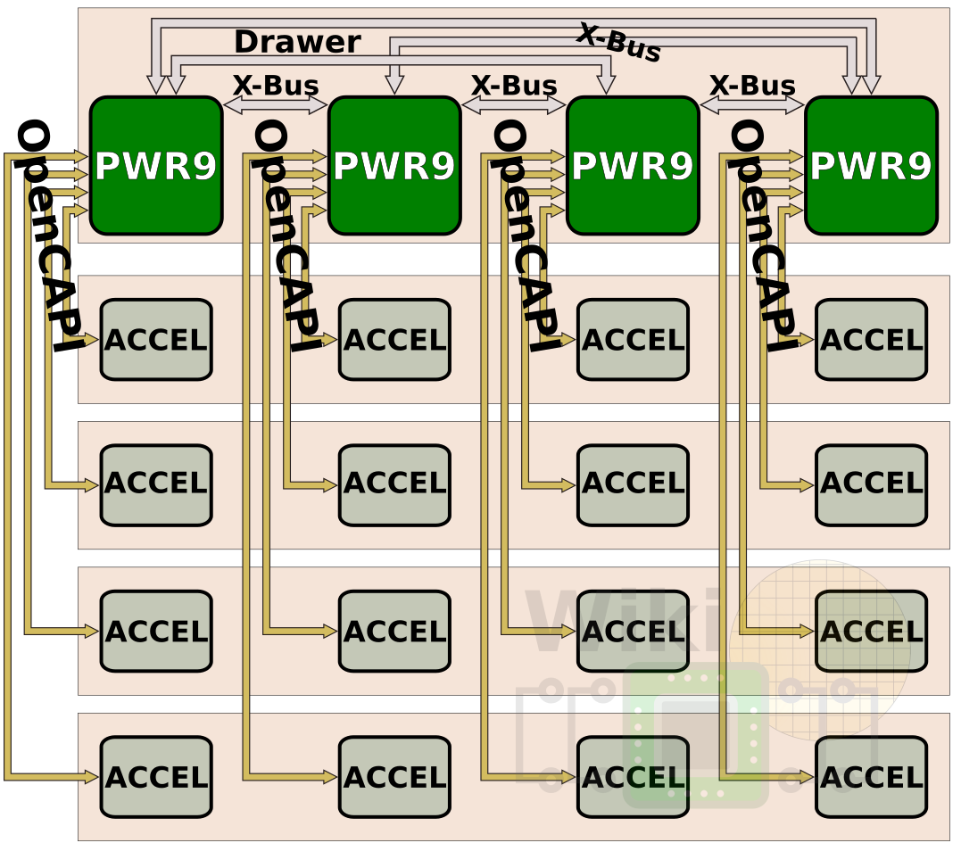
An example of their 16-socket server is the Power E980. Those are broken down into 4 5U nodes or drawers. Each drawer has four POWER9 processors in a 4-way configuration allowing for a full system with up to 192 cores along with up to 64 TiB of DDR4 memory, 32 PCIe Gen4 slots, and PowerAXON links for additional accelerators.
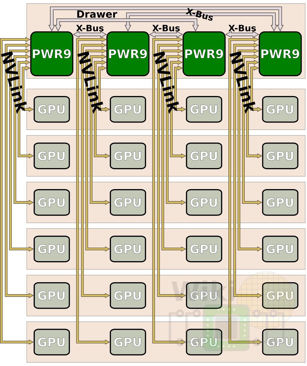
Although they don’t currently have such systems, Stuecheli showed a couple of forward-looking possible configurations. Making use of the PowerAXON again, one possible use is an array of 4x 6 GPUs communicating over six x8 NVLink 2.0 links. Alternatively, making use of OpenCAPI, the same box can be used for other accelerators such as FPGAs or storage-class memories.
|
|
OpenCAPI Memory For The Future
One of the arguments IBM makes is that the I/O infrastructure will become very important, perhaps more critical than the CPU itself. Accelerators such as the Nvidia V100 GPU in the Summit supercomputer get significant speed-up due to the coherency and large bandwidth between the accelerator itself and the host CPU. Likewise, in-memory databases enjoy similar performance improvements due to the large memory bandwidth offered by the buffered memory.

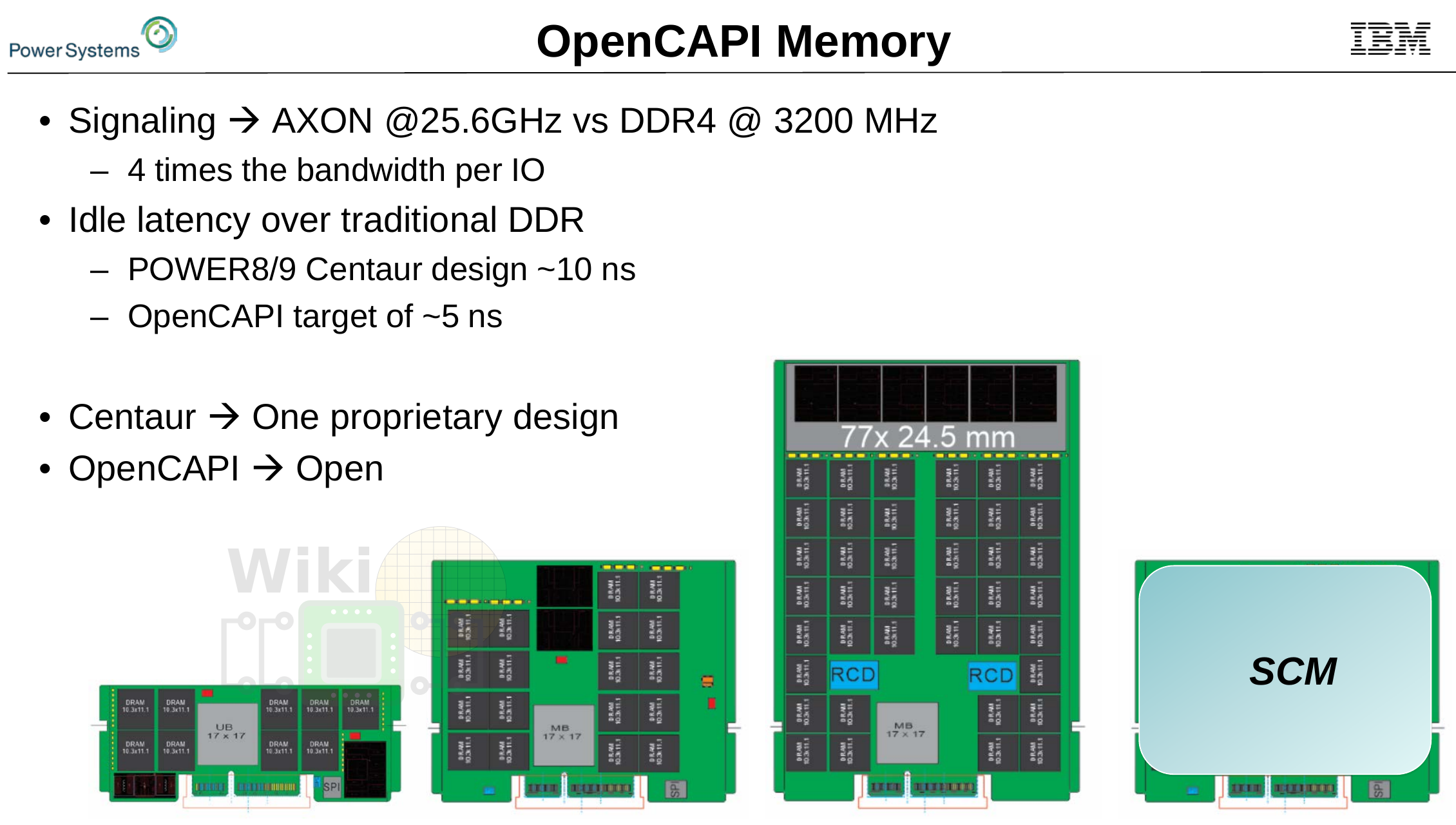
For those reasons, IBM wants to offer their buffered memory solutions to their scale-out processors as well. Centaur works well but IBM sees room for improvement. Whereas Centaur relies on their proprietary design (and their DMI channels), they have since been working on a JEDEC standard for a very low-latency OpenCAPI Memory. In many ways, OpenCAPI Memory generalizes Centaur. This is a memory-agnostic interface with no specific ties to any type of memory. Inherently, there is more flexibility here by offering pluggable memory such as DRAM, high-bandwidth, as well as SCMs, depending on the tradeoffs you’re willing to make.
Centaur had 1 interface going to four DDR ports with a 16 MiB cache lookup. This new chip is a single interface with a single port and no cache. Compared to Centaur, which had a 10 ns latency delay over direct-attached DDR, the current prototype being worked on is targetting roughly 5 ns.
Looking forward to next year, IBM plans a third POWER9 derivative which will replace their differential memory interface (DMI) with the OpenCAPI memory interface (OMI). Those processors are expected to feature around 350 GB/s per socket or 1.66x the memory bandwidth of their current Centaur-based buffered memory along with an upgraded interconnects providing support for NVLink 3.0 which has not been disclosed yet.
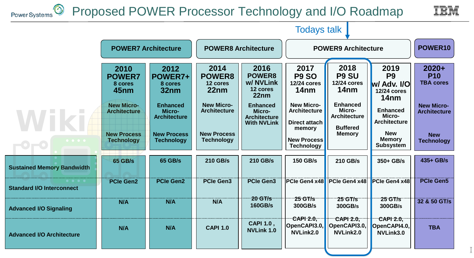
Their next major revision is POWER10 which is expected to feature PCIe Gen 5 and increase the memory bandwidth further to 435 GB/s. Those processors look to bump the signaling rate from 25 GT/s to 33 GT/s and even 50 GT/s.
–
Spotted an error? Help us fix it! Simply select the problematic text and press Ctrl+Enter to notify us.
–