
A Look At The ET-SoC-1, Esperanto’s Massively Multi-Core RISC-V Approach To AI
This article was originally published on May 16, 2021, as part of our Subscriber-Only Content. The paywall decayed on July 10. It is now viewable by everyone.
 Ask ten different engineers how they would design an AI accelerator and you’ll get ten different ways to arrange the billions of transistors on a modern leading-edge chip. With someone such as Dave Ditzel leading the project with his rich history of CPU design, it’s no wonder that Esperanto Technologies’ twist on machine learning chip design will somehow involve CPUs. And if one custom CPU isn’t enough, how about two designs? And with a budget of nearly 24 billion transistors, Esperanto managed to pack nearly 1,100 of them on their first AI accelerator – the ET-SoC-1.
The ET-SoC-1 – which stands for the “Esperanto Technologies Supercomputer-on-Chip 1” – targets the hyperscaler datacenter market and is the first product from a family of new AI accelerators by Esperanto. The ET-SoC-1 is an inference accelerator, not training. And while the design is complete, as of earlier this year, the company has yet to see first silicon. When we first talked about Esperanto exiting stealth mode, the timeline discussed was ~2020 timeframe. Development schedules have clearly slipped and if the new timeline holds, silicon should be back this quarter and production can be expected in early 2022. A two-year delay is rather costly when other AI startups have had production silicon sampling for over a year. Nonetheless, Esperanto is finally ready to share technical details of the new chip. It’s also worth pointing out that Dave Ditzel will be presenting the ET-SoC-1 at the upcoming Hot Chips 33 conference in August.
Some initial performance claims were made by Art Swift, Esperanto Technologies CEO. Swift stated that “we expect to deliver up to 50 times better performance on key workloads such as recommendation networks and up to 30 times better performance for image classifications.” The claims refer to full-chip emulation of the ET-SoC-1 versus measured inference benchmark results for “incumbent competitor in the data center”. “But probably more exciting and more important is the energy efficiency which we are able to derive. We expect to see 100 times better energy efficiency in terms of inferences per watt versus the incumbent solutions,” he added. The overly broad performance statements must be taken with a grain of salt, but Esperanto says we can expect to see published characterized silicon results in the near future.
Tile Up
Esperanto uses a very regular design based on a tiled architecture. The chip uses the company’s custom-designed RISC-V-compliant CPU cores, it uses standard DDR4 memory with a traditional memory hierarchy, and it leverages all the available RISC-V software ecosystem. In other words, for all practical purposes, the ET-SoC-1 passes the Duck Test as a standard RISC-V server CPU, albeit with lots and lots of simple cores that wouldn’t do too great on general workloads. In fact, Esperanto argues that their solution is very much future-proof for that very reason. Incorporating a large array of CPUs, the company says it can scale from hundreds to thousands of cores. In fact, since the ET-SoC-1 is designed for the data center, for lower-power applications such as edge inference, we can probably expect an identical cut down version of the ET-SoC-1. When Esperanto first started talking about their design at an extremely high level, they theorized a chip 4x the number of cores as the ET-SoC-1 we’ll be talking about in this article. It’s not outside the realm of capabilities for Esperanto to scale up the ET-SoC-1 in such a direction if their design proves itself.
Custom Cores
Esperanto went the RISC-V route. They design two custom cores – ET-Minion and ET-Maxion. As their names suggest, the ET-Maxion is your typical big core design capable of running a standard operating system such as Linux. Likewise, the ET-Minion is a workhorse small CPU with custom tensor extension for processing operations such as matrix multiplications. In the context of the ET-SoC-1, the ET-Maxion are used as control CPUs while the ET-Minions do the heavy data processing.
ET-Maxion
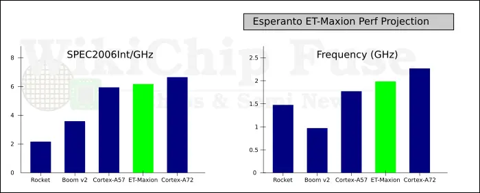
As we mentioned before, the ET-Maxion is a custom high-performance big core design. It was designed specifically for TSMC’s 7nm and with frequencies of over 2 GHz. The ET-Maxion is actually a fork of the UC Berkeley Out-of-Order Machine (BOOM) v2 CPU, however so much has changed/improved upon to make it more competitive and commercial-quality that the lineage is almost unrecognizable at this point. In fact, Chris Celio who developed BOOM moved on to Esperanto to work on the ET-Maxion (although since 2020 he joined Intel as a CPU Architect). When compared to BOOM, the ET-Maxion touched every aspect of the machine. It’s considerably wider, longer, and bigger. The entire front-end was redesigned and various execution units were rearchitected. It features new contemporary state-of-the-art branch predictors and prefetchers. There are new ground-up caches and TLBs with ECC support. And finally, Esperanto added commercial-grade silicon debug and performance monitoring capabilities. In terms of performance, the ET-Maxion is said to be slightly behind the Cortex-A72 at ISO-frequency on SPEC2006, but ahead of the Cortex-A57. Prior to SiFive’s recent announcement, the ET-Maxion would have likely been the highest-performance core available in the RISC-V world. Recently, SiFive introduced its P550 core which is said to deliver a SPECInt 2006 score of 8.65/GHz, significantly out-performing the ET-Maxion (and the A72) in IPC.
The ET-Maxion is an out-of-order CPU core with a 10-stage pipeline. The core is a four-wide machine – capable of fetching 16B each cycle, decoding them, and dispatching them to the back end at a rate of 4 instructions per cycle. Instructions are fetched from a 32 KiB banked instruction cache with parity and ECC support. Esperanto says that considerable effort was put into a new state-of-the-art conditional predictor and a path-based indirect predictor backed by a 2K-entry compressed BTB. The branch predictor comprises a two-level predictor. A fast, single-cycle BTB-based predictor performs the initial guess which gets backed up by a second level, slower multi-cycle, high accuracy branch predictor which may override it.
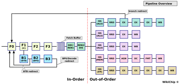
Each cycle, up to four instructions may be dispatched to the schedulers. The ET-Maxion uses a distributed scheduler design with a total capacity of 64 entries. There’s one scheduler for the LSU, one for the FPU, one for complex ALU, and one for simple ALUs. Note that there are two simple ALUs and the complex ALU unit is also capable of handling branch operations.
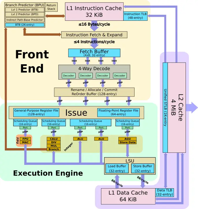
The execution units are fed by a 64-entry floating-point physical register file and a 128-entry integer physical register file. On the execution units side, the machine is five-wide with two simple integer units sitting on a single scheduler. Each cycle, up to five instructions may be scheduled for execution. The floating-point unit is 64b-wide and fully supports the RISC-V 32-bit (F) and 64-bit (D) floating-point extensions. Overall, the core is upper-bound by its 128-entry reorder buffer which, as with the front end of the machine, is capable of retiring up to four instructions per cycle.
| Microarchitecture Comparison | ||||
|---|---|---|---|---|
| Designer | Intel | Esperanto | Arm | AMD |
| uArch | Haswell | ET-Maxion | Maya (A72) | Zen |
| Scheduler | 60 | 64 [4×16] | 64 [8×8] | 180 [6×14+96] |
| EUs | 8 | 5 | 8 | 10 |
| ROB | 192 | 128 | 128 | 192 |
| In-flight LDs | 72 | 32 | ? | 72 |
| In-flight STs | 42 | 32 | ? | 44 |
| I PRF | 168 | 128 | ? | 168 |
| FP PRF | 168 | 64 | ? | 160 |
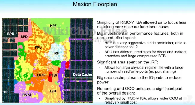
Esperanto initially considered a custom ISA but eventually sattled on RISC-V due to its simplicity. The company explained that the simple architecture allowed them to focus more of their effort on performance features rather than working out corner cases and quirks with other ISAs. A floorplan of the ET-Maxion is shown below. Note that this is core without the L2 shown. From the die plot, it can be seen that considerable area was spent on the cache arrays (almost 1/3 of the area) and the branch prediction unit. At the top of the core is the hardware prefetcher (HPF) (L1 only) which is extremely large by comparison to other components. The choice to go with a more aggressive (and slower but more accurate) prefetcher allowed them to place it at the top and outside of the critical path, simplifying wiring.
ET-Minion
The ET-Minion is the second custom CPU core from Esperanto. This one is quite a bit different from the previous one and is a bit more interesting. The ET-Minion is also a 64-bit RISC-V processor but this one is an in-order machine. Since this is a throughput-oriented core, it’s also multi-threaded with two threads that can be alternated on stalls. The ET-Minion features a pipelined scalar design – fetching, decoding, and issuing a single instruction per cycle. (Note that the diagram below may have some missing details as Esperanto mainly discussed the vector capabilities of the core).
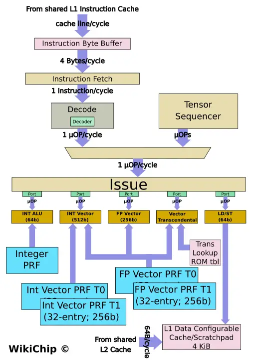
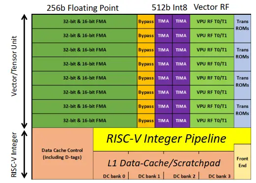
Aimed at inference acceleration, Esperanto’s hidden weapon is the execution engine of the ET-Minion. The backend on the ET-Minion is vector-heavy and there is just a single execution unit for performing all the necessary (64b) operations required by the RISC-V architecture. The bulk of the core comprises the two vector pipelines. There is a 256b floating-point vector unit and a 512b integer vector unit. Accompanying those vector units are two register files – a 32-entry 256b FP register file and a 32-entry 256b integer register file. Note that those register files are duplicated for each thread (i.e., 64 entries in total ea). The FP vector unit is subdivided into 8×32-bit FMAs capable of performing up to 16 SP FLOPs/cycle or 32 HF FLOPs/cycle. The integer vector unit is 512b wide, twice as much as the FP vector unit. This unit is subdivided into 16×32-bit TIMAs capable of performing up to 128 INT8 OPs/cycle. While the FP vector unit can be fed from the FP vector register file, the integer vector unit, which is twice as wide, requires fetching half of the vector (256b) from the FP vector register file and the other half from its own private integer register file (256b) for the combined 512-wide vector.
Esperanto packed a lot of floating-point horsepower into the ET-Minion which is a striking contrast to other contemporary accelerators. Normally we see accelerators that offer only INT8 operations. While you can get pretty good levels of fidelity from 8-bit quantization, Esperanto does have an edge for workloads where FP16 (or 32) are desired.
In addition to the vector units, the ET-Minion incorporates a vector transcendental unit that can perform transcendental functions such as the various trigonometric functions, exponentials, and logarithms for speeding up things such as activation functions. The trans unit is ROM-based, favoring lower power over silicon. There are a number of other nuances to the vector units here. In addition to standard RISC-V instructions, Esperanto implemented its own instruction extension – two of them. They added multi-cycle tensor instructions and accompanying vector transcendental instructions. This is a move that some of our readers will find a bit unnerving, especially since Esperanto talked up the benefits of RISC-V so much. But the reality is that RISC-V, like all other ISAs, doesn’t have any specific instructions for accelerating AI and such extensions are a necessary evil. In fact, the RISC-V Foundation foresaw this and baked custom extensions right into the specs which is why Espernato can do this in a standard way. It’s unclear if Esperanto will publically disclose its extension or if they plan on keeping it proprietary as it goes against their claim of being future-proof.
The multi-cycle tensor instructions allow the core to read a single instruction and, through the use of a Tensor Sequencer state machine, it can replay a series of operations over 100s and even 1000s of cycles. As with most sequencers, the ET-Minion clock gates the entire front end and every other unit that’s not utilized when the tensor operations are being issued and executed. This allows the core to further cut down on power.
By the way, the ET-Minion physical design is quite unique on its own. The pipeline was designed with a low gate count per stage in order to improve the frequency at low voltage. Esperanto has gone further and designed its own custom SRAM instead of using TSMC’s standard SRAM offering. The cells, while physically larger, can stably operate at considerably lower voltage – far below nominal. “When I talk about low voltage operations, I really mean operating at much lower than nominal voltages. So, if nominal is 0.75 V or so, we are operating on the order of 400 mV,” Swift said.
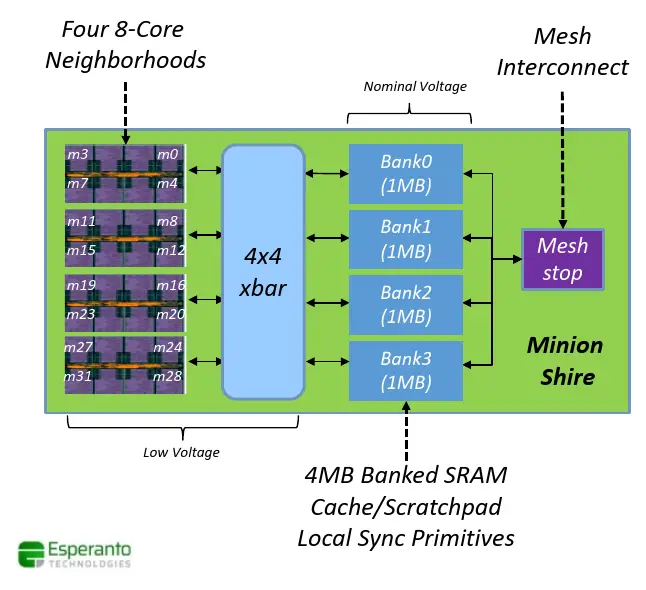
The Minion Neighborhood
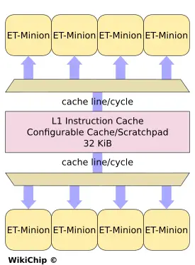
Group eight ET-Minions together and you get what Esperanto calls a Minion Neighborhood. Within a neighborhood, each core competitively shares the instruction cache. The capacity of the cache is 32 KiB. Each cycle, a cache line is sent to two cores. In other words, the instruction cache round-robins a pair of cores on each cycle, sending 64B (16 instructions worth) to two separate cores. The cores buffers the line, allowing them to continue to operate as the instruction cache moves on to feeding other cores.
The Minion Shire
Four neighborhoods are then grouped together into a Minion Shire for a total of 32 cores. Each octa-core neighborhood is connected to four banks of L2 memory through a crossbar. The L2 comprises four 1 MiB SRAM banks that are software configurable as cache or scratchpad memory. Under the scratchpad configuration, the entire memory is one large address space that can be used by software to organize the data in the precise way it will be used and access it as such. Interestingly, the L2 cache – which by default is private to each individual Minion Shire – can also be configured as a last-level cache that can span the entire chip. And all those functionalities are offered on a per-bank granularity. For example, one bank may be reserved as a scratchpad memory while another bank is used for a 1 MiB/Shire LLC and the other two banks can be configured as 2 MiB of private L2 cache. Each Shire can communicate with other Shires through a mesh interconnect with a single mesh stop per Minion Shire.
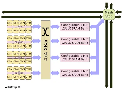
Due to the low-voltage design of the ET-Minion, the neighborhoods along with the crossbar sit on their own low-voltage power plane within the Shire. The rest of the Shire (e.g., banked SRAM and mesh interconnect components) sit on the standard voltage plane.
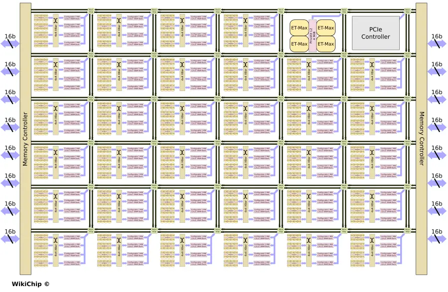
Tiled Architecture
The tile design is straightforward, each Minion Shire is connected to any other Shire and any other component on the chip through the mesh stop. The mesh stops incorporate two unidirectional links in each of the four cardinal directions. Those links appear to be 1,024b wide each. Esperanto has a number of additional components on the chip such as memory channels and a PCIe interface which are also connected via their own mesh stops into the overall mesh interconnect.
The ET-SoC-1
All of that finally leads us to Esperanto’s first product – the ET-SoC-1. This chip integrates 34 Minion Shires in a grid of 6×6. The two additional tiles on the grid are for a control processor cluster and a PCIe tile. The 34 Minion Shires mean there are 1,088 ET-Minion processors on-die along with 136 MiB of configurable L2 memory. There is actually one additional independent ET-Minion that acts as a service processor. Finally, the ET-SoC-1 integrates a quad-core ET-Maxion tile with 4 MiB of private L2 which can be used as a self-hosting processor (e.g., running Linux). While the ET-SoC-1 targets the hyperscaler datacenter market which means it sits along a higher-performance server processor, for edge applications, the ET-Maxions will play a bigger role in enabling full high-performance operability.
The chip is fed through a low-power LPDDR4x 16x16b (256b) interface. The DRAM controller supports 32 GiB of DRAM at 137 GB/s. All in all, the ET-SoC-1 features 1,093 (1088+1+4) cores and interfaces with the outside world with x8 PCIe Gen4. The Chip is said to have a typical operating power of around or under 20 Watts, which allows Esperanto to fit within the specs of the OCP M.2 Accelerator Module. We also expect higher-power PCIe cards to be made available.
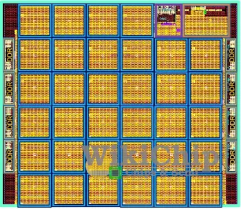
Physically, the chip is fabricated on TSMC’s N7 process technology. Esperanto did not disclose the die size, but packing 23.8 billion transistors, it’s likely north of 350 squared millimeters. Although it can reach 1.5 GHz, nominally, the chip target frequency is around 1 GHz for their 20 W power target. A single ET-Minion is capable of 128 OPS (INT8)/cycle or 128 GOPS at 1 GHz. Assuming all 1,088 ET-Minions are doing peak useful work. At 1 GHz, we’re looking at 139.3 TOPS (INT8) of peak theoretical compute for the entire chip. At 1.5 GHz, that’s increased to 208.9 TOPS. Unlike many other accelerators, the ET-Minions also support full 32b and 16b floating-point operations as well. Therefore, at 1 GHz, the ET-SoC-1 is also capable of nearly 35 teraFLOPS (half precision) of peak compute if FP16 is desired. At 1.5 GHz, that gets bumped up to 52.22 teraFLOPS.
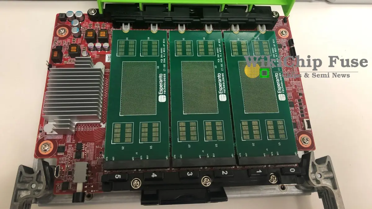
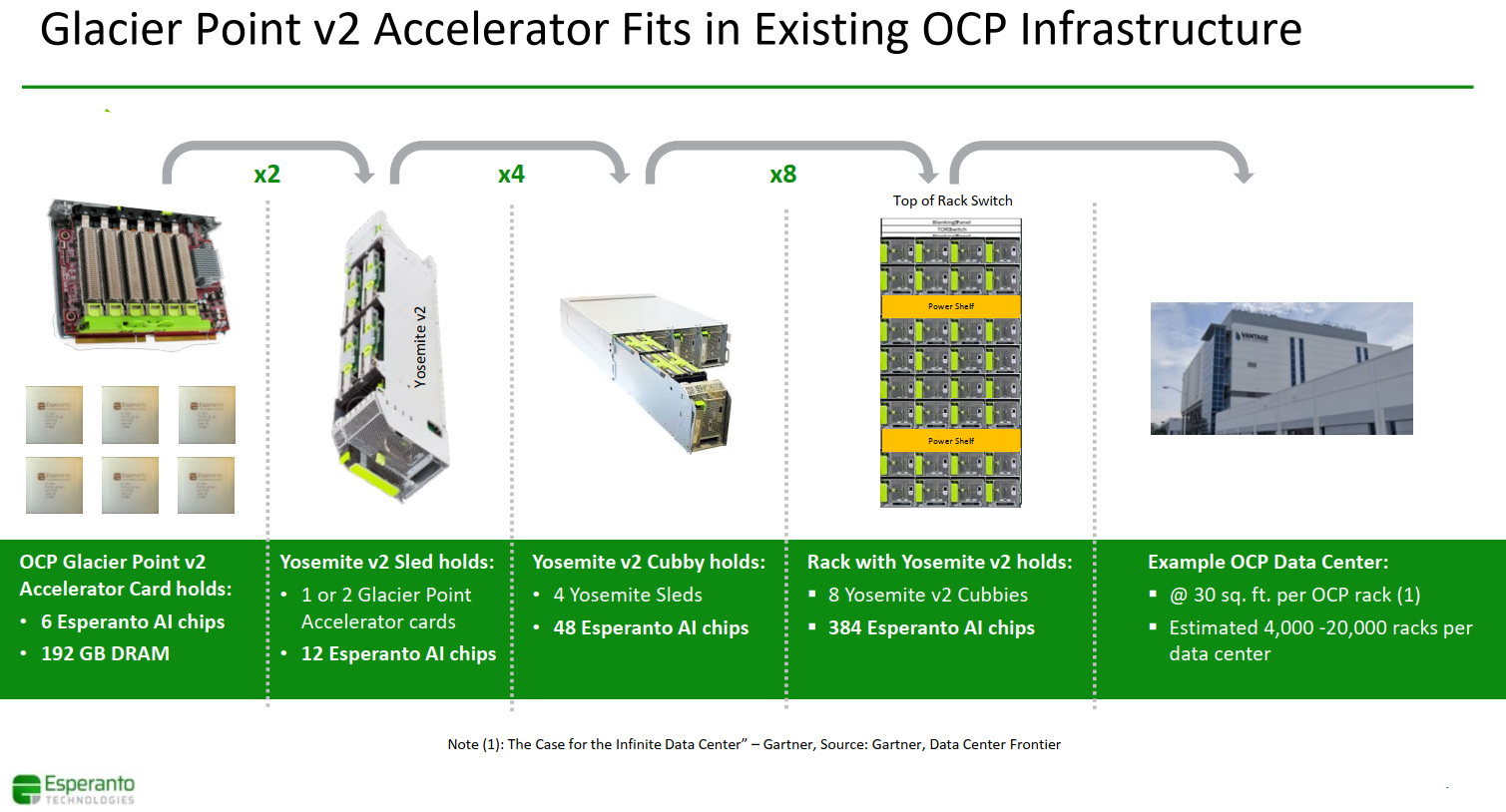
OCP Glacier Point V2 Card With 6x ET-SoC-1 Chips
Since the chip fits within the OCP M.2 Accelerator Module, Esperanto suggests it can pack six Esperanto Dual M.2 Accelerator Modules (three on top and three on bottom) of the OCP Glacier Point V2 Card. Those are designed to plug right into the OCP Yosemite v2 multi-node server platform. With six modules, each Glacier Point card will have 6,558 RISC-V cores along with 192 GiB of LPDDR4x memory with 822 GB/s of DRAM bandwidth. At peak theoretical performance, the card can achieve 835.6 TOPS (INT8) or nearly 210 teraFLOPS (half precision).
Once Esperanto gets its silicon back, we should start hearing more detailed performance claims. As we mentioned early on, Dave Ditzel will be presenting the ET-SoC-1 at the upcoming Hot Chips 33 conference in August where they might disclose more technical details and benchmarks.
–
Spotted an error? Help us fix it! Simply select the problematic text and press Ctrl+Enter to notify us.
–