
Samsung 3nm GAAFET Enters Risk Production; Discusses Next-Gen Improvements
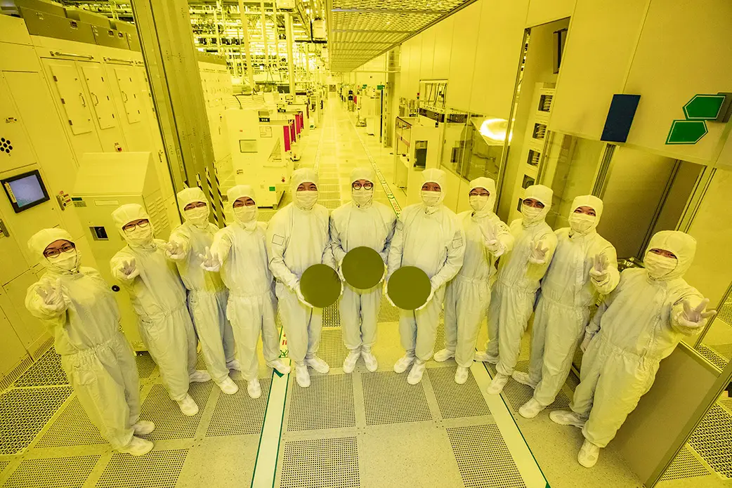
Last week Samsung Foundry announced its 3-nanometer node has entered risk production. The announcement marks a significant milestone for both Samsung and the semiconductor industry.
3nm GAA
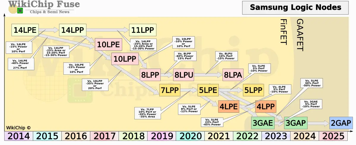
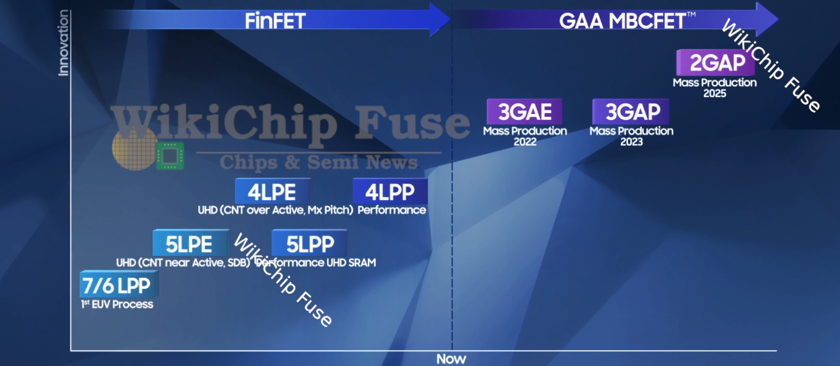
Samsung’s latest process technology in production is their 4nm node. That node ramped-up production late last year. This is their last FinFET-based leading-edge process technology – albeit not the last one they plan to introduce altogether. Moving forward the company’s future leading-edge technology nodes will utilize a new GAA FET device architecture. Samsung Foundry has two flavors of their 3nm GAA process planned – 3GAE and 3GAP.
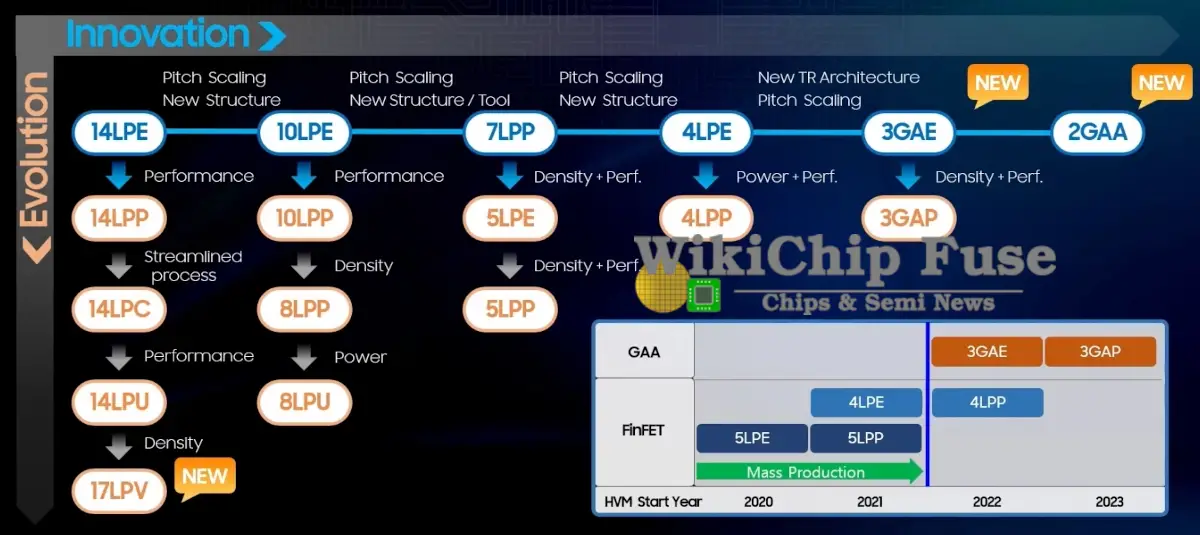
The first-generation – 3GAE – has entered risk production and will reach mass production by the end of the year and into 2023. Compared to their 5nm process technology, 3GAE can reduce power by up to 45%, improve performance by 23%, and reduce the area by 16%.
The company’s second-generation – 3GAP – is expected to be a fast-follow, entering mass production by the end of next year. Samsung says that compared to the same 5nm process as 3GAE, 3GAP will offer a power reduction of up to 50%, improve performance by 30%, and reduce the area by 35%. In other words, compared to 3GAE, 3GAP should offer roughly up to 10% power reduction, 5.5% performance improvement, and 22% reduction in area. Samsung didn’t explicitly state which 5nm node they were comparing to. The company rolled out a 5LPE process which was followed by 5LPP. However, historically, Samsung compared new nodes with their first-generation versions (e.g., 4LPE was compared to 5LPE, and 5LPE was compared to 7LPE). Therefore, we will assume that 3GAE/P is no exception and those PPA claims are stated against first-generation 5nm, 5LPE.
Several things stick out right away. In terms of power, the transition from FinFET to GAA produced a claimed power reduction of up to 50%. For Samsung Foundry, we haven’t seen such large power reduction claims since the days of planar transistors. On the other hand, in terms of performance, those numbers are on the high side, but only slightly higher than some of the prior nodes. For 2nd-generation, 3GAP, the performance and power numbers are largely in-line with what we expect for a follow-up node, not too dissimilar to 5LPP or 4LPP.
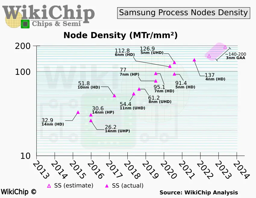
3GAP clearly aims at boosting area scaling rather than introducing any major performance/power improvements. This is what we would expect to see. An initial roll-out of a new transistor architecture with conservative scaling or no scaling at all, followed up by device refinement and address scaling. Translating area reduction into transistor density, it works out to a roughly 1.2x density improvement for first-generation 3GAE which is then increased to 1.54x (still over 5nm) for 3GAP which aligns much more closely to a full node worth of density for Samsung.
Given we don’t have any actual data on the process, it’s hard to put an exact number but a rough estimate puts 3GAE at around 150 MTr/mm² with 3GAP at around 195 MTr/mm². For now, we’ll put a rough estimate ‘zone’ of around 140-200 MTr/mm² for 3GAE and 3GAP. We’ll be able to know more accurately determine those numbers ones the company starts disclosing more information about the process itself and various design rules. Roughly speaking, Samsung’s 3GAE will surpass TSMC’s N5, but it’s entirely possible it will tie in terms of density against N4. Looking ahead into next year, 3GAP might be fairly comparable to TSMC’s N3 node.
For more technical details on Samsung’s 3nm GAA process, we’ll have to wait for their conference presentations.
3 Nanosheets, Varying Widths
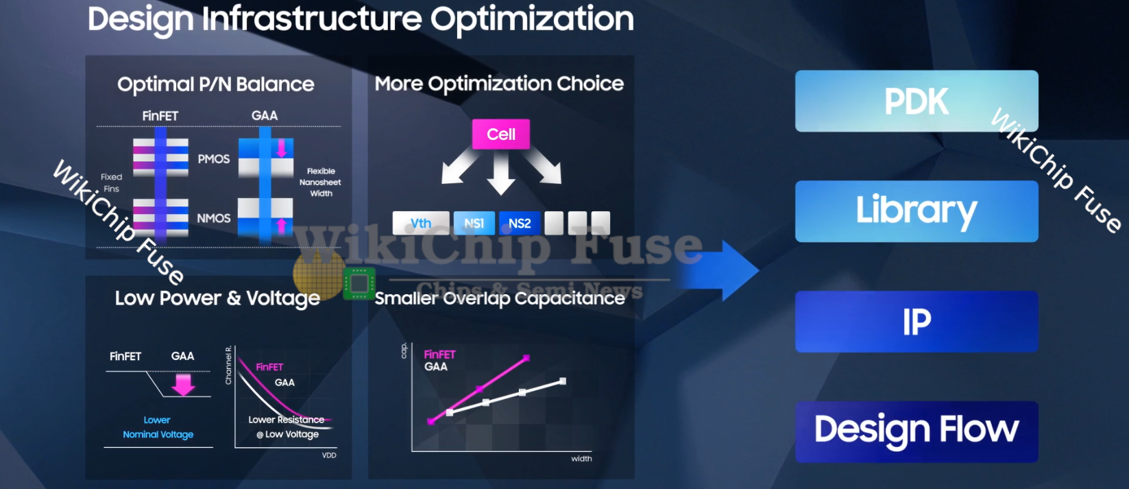
Samsung calls their transistors Multi-Bridge-Channel FETs (MBCFETs), their own flavor of nanosheets. So how many nanosheets does Samsung’s 3nm have? The answer is 3. Their initial 3-nanometer process technology will feature 3 stacked nanosheets. Whereas previously, on FinFET-based nodes, the PPA of cells was quantized based on the number of fins in the cell, on 3GAA, the three sheets are fixed, however, performance can be fine-tuned via the gate width for an infinite theoretical PPA gradiant. Samsung has talked about four predefined nanosheet widths that offer a tradeoff between density and performance.
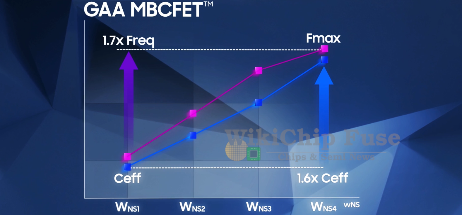
The widest nanosheet variant offers 1.7x the frequency at 1.6x added capacitance. Samsung says that this is a better improvement than the FinFET multiple fins equivalent.
2nm and Timeline
Samsung expects 3GAE to ramp throughout this year with mobile processor production going into 2023. 3GAP will be a refined version of 3GAE and will quickly ramp towards the end of next year. Samsung says that it hopes to transfer all its production knowledge from 3nm to 2nm. To that end, Samsung says it expects 2nm to ramp two years after 3GAP. Their 2-nanometer node is called 2GAP and is planned to enter mass production in 2025.
Samsung says that 2GAP will include pitch scaling for improved transistor density. Additionally, 2GAP will add another nanosheet for a total of four stacked nanosheets in order to improve drive current.
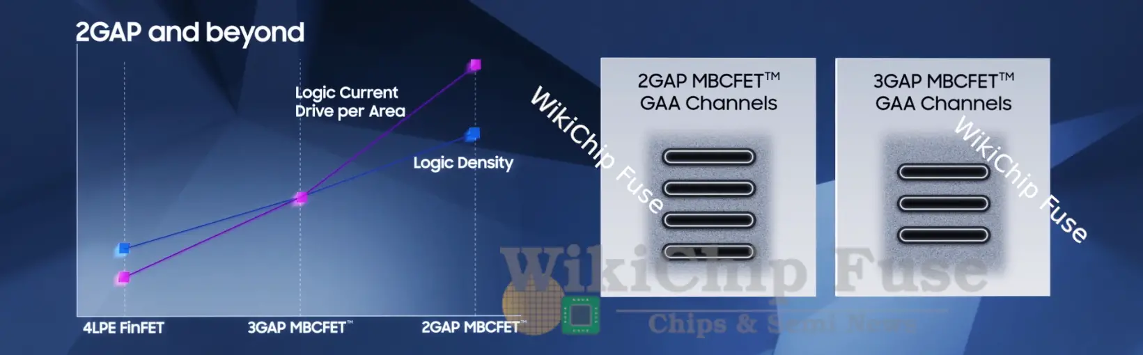
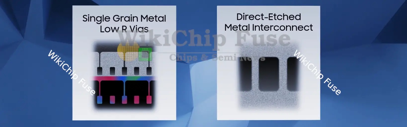
Samsung says that they are working on a number of metallization stack improvements for 2GAP and beyond including single grain metal for low resistance and direct etched metal interconnect.
–
Spotted an error? Help us fix it! Simply select the problematic text and press Ctrl+Enter to notify us.
–