
DARPA ERI: How Ayar Labs Collaboration With GF Produces A Photonics Chiplet That Can Supercharge Intel FPGAs
Earlier this week, DARPA hosted the second annual Electronics Resurgence Initiative (ERI) Summit. One of the interesting announcements that came out of the ERI Summit was a new partnership by Intel with two startups that extend the functionality of Intel’s FPGAs through custom, high-performance, chiplets. This includes very high bandwidth photonics transceivers as well as high-end RF capabilities.
A Brief History: DARPA Seed Effort
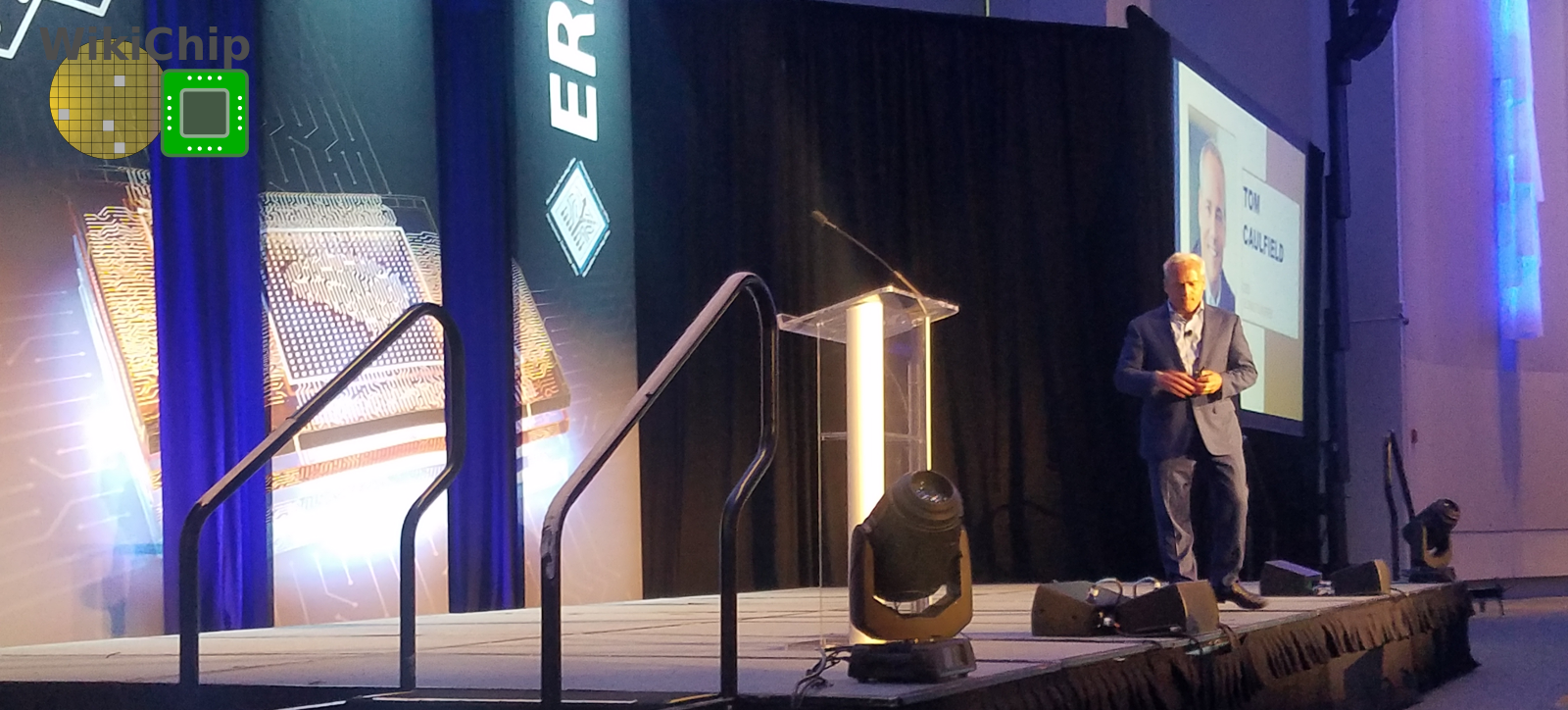
To see how they got here, you have to go back. Almost a decade back. At the Summit, Dr. Thomas Caulfield, GlobalFoundries CEO, gave a keynote about the company’s differentiation strategy and how they align with DARPA’s mission. “They [DARPA] understand future needs. They set ambitious goals. So if the world is communicating at a gigabit today, they will say we want a terabit. And they will fund it on a pragmatic timeline,†Caulfield said. “So it’s a springboard not only to serve national security; it’s a springboard to create the commercialization of technologies,†he added.
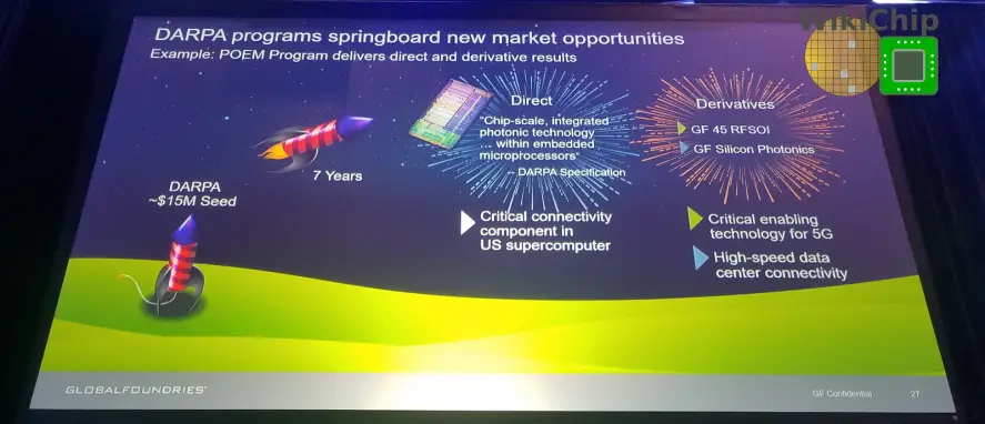
One such example is the Photonically Optimized Embedded Microprocessors (POEM) program. POEM is the successor to an earlier DARPA program called Ultraperformance Nanophotonic Intrachip Communications (UNIC). In a way, POEM is the successful realization of a long-term goal DARPA had of integrating photonics in a microprocessor for intra-chip and inter-chip photonic communications.
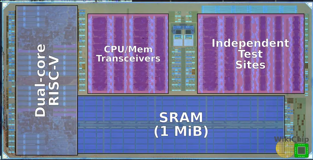
Under POEM, a group of researchers designed and developed the first microprocessor chip to communicate using light. The end result was a single chip with over 70 million transistors that incorporated 850 photonic components. The chip incorporated a dual-core RISC-V microprocessor, based on Rocket, along with 1 MiB of SRAM. The chip features two optic transceivers sets – one set for the CPUs and one for the memory. Within each set, there were two receiver banks with eleven receiver sites and two transmitter banks with eleven transmitter sites. Fabricated on an unmodified foundry 45 nanometer CMOS SOI process, the researchers were able to successfully demonstrate proper operation.
Many of the POEM chip researchers went on to form a startup called Ayar Labs.
Caulfield explained that the POEM program resulted in an optimized process at GlobalFoundries called 45RFSOI. “RFSOI is instrumental to 5G millimeter wave deployment, “ Caulfield said. “The silicon photonics part of that process is designed for high-speed data center connectivity,†Caulfield added. In 2017 GlobalFoundries announced a collaboration with Ayar Labs intended to accelerate the commercialization of CMOS optical I/O technology using this process.
A Validation of the Technology, DARPA CHIPS, And Intel Chiplet Ecosystem Effort
An entirely different program known as the Common Heterogeneous Integration and IP Reuse Strategies (CHIPS) program is currently running. CHIPS is part of the Electronics Resurgence Initiative (ERI). CHIPS vision is quite extraordinary – creating an industry-wide ecosystem of discrete modular, reusable IP blocks, which can be assembled into systems using existing and emerging integration technologies. In other words, an industry-driven, compatible chiplet ecosystem, whereby designers can mix and match the desired chiplets from many different vendors based on their specific needs forming more customized solutions with less engineering resources and faster time-to-market.
CHIPS is headed by Andreas Olofsson who gave an update on the program at the summit. A detailed summary will be published in a future article. As part of CHIPS, Intel has been using their FPGA platform as a way of commercially experimenting with the concept of chiplets and a chiplet ecosystem. Last year, Intel released the advanced interface bus (AIB) interconnect as a royalty-free interconnect standard for chiplet architectures. At the summit, principal investigator from Intel to CHIPS and Senior Principal Engineer, Sergey Shumarayev, gave an update on their work as part of the program.
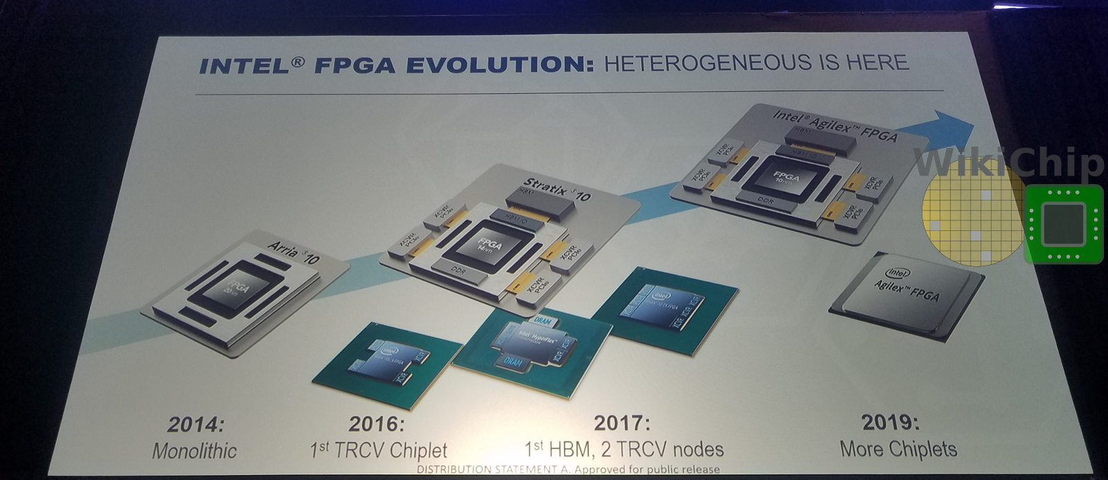
Intel’s last monolithic FPGA was the Arria 10. They moved to a chiplet-based solution in 2016 with the introduction of the Stratix 10 series. The Stratix 10 can integrate many different chiplets through the AIB interface. Chiplets are physically integrated into the package using the company’s EMIB solution. First generation Stratix 10 FPGAs integrated transceiver chiplets only. By 2017, they started integrating HBM as well as transceivers from different process nods from different foundries. Earlier this year, Intel introduced the Agilex FPGA family based on their 10-nanometer node which will start to lead customers soon. Agilex uses the same AIB interface as the Stratix 10, allowing existing chiplets to work seamlessly with the new FPGA family.
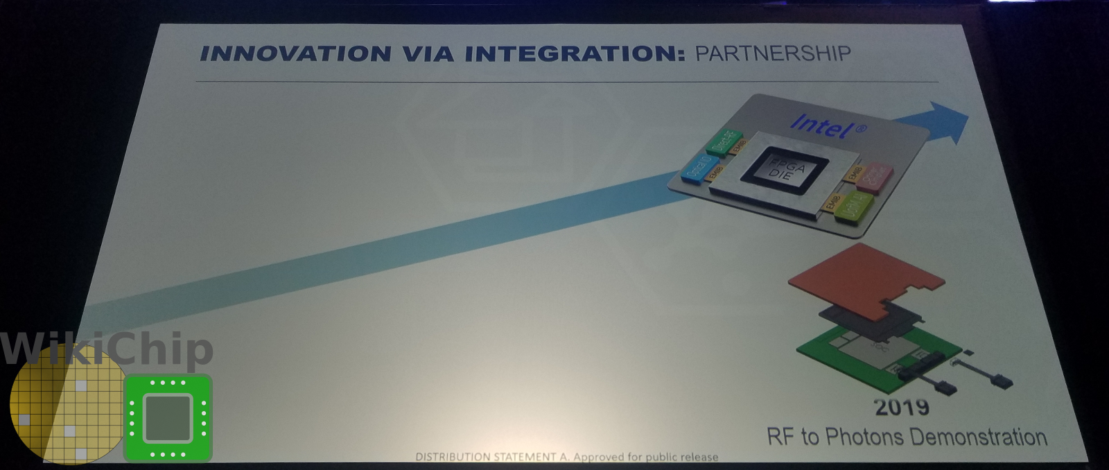
Shumarayev said that Intel has been experimenting with more chiplets and other unique functionalities internally but they were also looking to broaden their options through external solutions. “If we could take this new commercial chiplet capability and come up with new killer applications for this program, we thought: wouldn’t it be nice to gain high-end RF capabilities on one side of the device which could be processed by the FPGA and be able to send it out optically on the other side, that would be a really awesome thing to do,†Shumarayev said. “And can we do it in a very short period of time with low NRE?†he added.
To that end, Shumarayev announced two new partnerships – Jariet Technologies and Ayar Labs. A new high-end direct-RF chiplet was designed by Jariet. Ayar Labs will be supplying the TeraPHY chiplet.
TeraPHY Chiplet
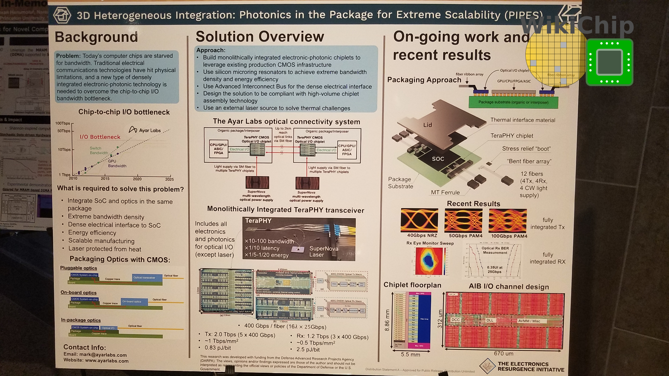
Intel and Ayar Labs will have a joint presentation at Hot Chips 31 next month. Ayar Labs presented a poster at the summit and we had the opportunity to chat with them. The TeraPHY chiplet connects to the FPGA just like any other chiplet via a wide AIB interface likely using an EMIB. Measuring just 48.73 mm², the chiplet packs three 400-gigabit receivers as well as five 400-gigabit transmitters. The transmitters comprises sixteen 25-gigabit wavelengths per fiber for a total of 2 Tbps with a data flux of ~1 Tbps/mm² at 0.83 pJ/bit. The receivers are at around ~0.5 Tbps/mm² with a power efficiency of 2.5 pJ/bit.
More information will be disclosed at Hot Chips 31 next month.
–
Spotted an error? Help us fix it! Simply select the problematic text and press Ctrl+Enter to notify us.
–