
TSMC To Build A 5-Nanometer Fab In Arizona; Invest $12B Over The Next 8 Years
![]()
TSMC announced today its intention to build and operate an advanced fab in Arizona. The announcement comes days after reports surfaced that the White House was in talks with Intel and TSMC to build new advanced fabs in the United States.
TSMC says the new fab will be built in Arizona “with the mutual understanding and commitment to support from the U.S. federal government and the State of Arizona.” The foundry will make use of TSMC’s very latest leading-edge 5-nanometer process and have a 20,000 monthly wafer start capacity. The company says it expects the facility to create over 1,600 jobs directly and thousands of indirect jobs in the semiconductor ecosystem.
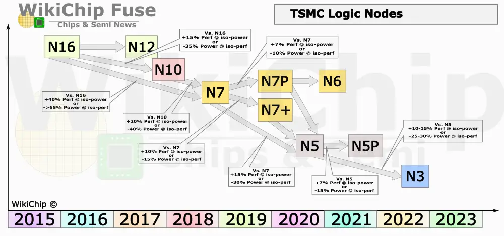
There are a few things to point out. First, the choice of Arizona is not unexpected. Arizona is a desert hub for a number of major semiconductor foundries including Intel’s currently under-construction EUV Giga Fab in Chandler, AZ where their 7-nanometer will be ramping next year. So there is already a robust semiconductor ecosystem in place. The capacity is by no means very high. In TSMC’s terms, it would be somewhere between a ‘mini’ and ‘mega’ in size. At 20K WPM, you are looking at a fab that will account for 1.6% of TSMC’s total wafer capacity (which is currently somewhere in the ballpark of 1.2M WPM 12″-eq). By comparison, TSMC’s current flagship fab, Fab 18, which recently ramped 5 nm has a capacity of well over 100,000 wafers per month. So we’re looking at a leading-edge fab with quite limited capacity.
The fab construction is planned for 2021 with production starting in 2024. The fab will technically be TSMC’s second fab in the United States as they already have a small 8-inch fab in Camas, Washington owned by their subsidiary WaferTech. If they stick to their schedule and their process node cadence remains on track, this fab will start production of 5nm when its main fab ramps production of its 3-nanometer process at their 12-inch GigaFab located at the Southern Taiwan Science Park, Taiwan. “TSMC’s total spending on this project, including capital expenditure, will be approximately US$12 billion from 2021 to 2029.”
“This U.S. facility not only enables us to better support our customers and partners, it also gives us more opportunities to attract global talents. This project is of critical, strategic importance to a vibrant and competitive U.S. semiconductor ecosystem that enables leading U.S. companies to fabricate their cutting-edge semiconductor products within the United States and benefit from the proximity of a world-class semiconductor foundry and ecosystem.”
Related Articles
- TSMC Ramps 5nm, Discloses 3nm to Pack Over a Quarter-Billion Transistors Per Square Millimeter
- TSMC Details 5 nm
- TSMC Q4: 7nm Dominates Revenue, Preps 5nm Ramp, 6nm By EOY
- TSMC N7+ EUV Process Starts Shipping
–
Spotted an error? Help us fix it! Simply select the problematic text and press Ctrl+Enter to notify us.
–