
Q1 2021 Foundry Update: Spending Bonanza
Amid the COVID-19 pandemic, chip shortage, and strenuous supply chain demands, the first quarter of 2021 was filled with new developments in the semiconductor manufacturing world. All three of the major leading-edge process manufacturers – Intel, TSMC, and Samsung – announced plans doubling down on future nodes and manufacturing capabilities. SMIC trailing behind.
Intel
By far the biggest headline mover this quarter was Intel. Pat Gelsinger, Intel’s new CEO, said in a recent interview on 60 Minutes that the company will no longer be focused on buyback going forward anywhere nearly as much as they were in the past. The statement comes amid heavy criticism regarding its spending strategy of buying its own stock versus more spending on R&D following nearly a half a decade of manufacturing woes.
At a virtual event in March, Gelsinger unveiled the company’s new “IDM 2.0” vision. At the event, Gelsinger reaffirmed their commitment to leading-edge manufacturing and chip design. Gelsinger stated that they had identified and resolved the issues with their next-generation 7-nanometer node slated for late 2022-2023. Originally planned for a less capable EUV ecosystem, the delays with 10-nanometer mean 7nm will now ramp with a production-ready EUV environment. This mismatch resulted in a more complex process not designed to make heavy use of EUV. Gelsinger noted that adjustments to the process were made to take full advantage of EUV, considerably simplifying their 7nm.
Last October Intel announced it will be selling its NAND chips business to memory company SK Hynix in a $9 billion deal. EU antitrust regulators have until this Thursday (May 20th) to weigh in on the deal. The deal already cleared the US FTC and the Committee on Foreign Investment. Additionally, Intel currently also has two separate ongoing lawsuits. An ongoing lawsuit alleges the company mislead investors when it discussed the state of its 7-nanometer process. The other lawsuit involves patent troll VLSI Technology which recently lost a $3.1 billion patent infringement lawsuit against Intel. The ruling comes just a month after Intel lost to VLSI in a separate ($2.2B) lawsuit which is being appealed.
As part of IDM 2.0, the company plans to become a global chip foundry for customers – opening up its factories in both the United States and Europe for customers. To that end, Intel created the Intel foundry services, a fully vertical, standalone foundry business unit. As part of their new foundry effort, the company announced two new major factories at their Ocotillo campus in Arizona with construction starting this year. Intel said the new expansion represents an investment of roughly $20 billion and creates over 3,000 new permanent high-paying fab jobs. Earlier this month Intel also announced its investing $3.5 billion to expand its Rio Rancho campus in New Mexico. Intel said it will invest to equip the NM campus for the manufacturing of advanced semiconductor packaging technologies, including its 3D packaging technology, Foveros. Construction is set for later this year and is expected to add 700 new jobs on campus.
As part of their new foundry, the company is looking to entice new customers through their added capacity. The company says it is in talks with automotive manufacturers and is looking to produce some of their chips within a year. It’s worth noting that the majority of those chips are not leading (or even trailing-edge) chips. Intel is also in negotiation with the European Union for a new fab as Europe looks to reduce its chip imports reliance. The company seeks around €8 billion ($9.25 billion) in subsidies.
Following the New Mexico announcement, Intel switched to Israel where Gelsinger stopped there for a tour of its Hifa Campus. From 2019 to 2021, the company invested $27 billion in US R&D and $17B in R&D in Ireland and Israel. Intel is also the largest private employer in Israel with nearly 15,000 employees. Intel said it will be investing $200 million to expand its Haifa campus known as Israel Development Center or IDC. IDC has been a major design center for Intel with many of the company’s most successful microarchitectures being developed there. The new expansion is for a massive new building across from the existing campus on the order of a few hundred thousand square feet housing thousands of engineers (mostly hardware, electrical, and AI). According to Israeli news sites, the new building is dubbed IDC12. The building is designed for a more hybrid office-remote work environment. The new campus is expected to add an additional 1,000 new engineers.
Intel also announced it will be investing an additional $400 million to turn its Jerusalem Mobileye center into a global R&D campus for self-driving car technology development. Intel acquired Mobileye in 2017 for more than $15.3 billion. In recent years Intel also acquired Israeli AI startup Habana in 2019 for $2 billion and Israeli mobility-as-a-service provider Moovit for $1 billion. During his tour, Intel confirmed that the first phase of its Fab 28 plant expansion has begun. The $11B expansion ($10B + $1B Israeli government grant) was announced in 2019 with the details confirmed in 2020. Fab 28, which is located at Kiryat Gat, is currently ramping up its 10-nanometer production.
TSMC
In early February TSMC’s board approved $11.8 billion for fab construction, installing and upgrading advanced packaging technology, and adding mature and specialty technology capacity. Earlier last month, TSMC approved an additional $2.9 billion to install additional mature technology capacity. The company also approved establishing a new $186 million R&D center in Japan. The new center primarily focuses on advanced packaging and testing.
TSMC saw multiple power outages this quarter. Last month, due to a construction accident, power was accidentally cut off. The company said the damaged line was repaired later the same day. Last week Taipower, Taiwan’s state-owned power company, experienced a power outage due to human error. The outage was said to affect some of TSMC’s facilities. Beyond those two incidents, Taiwan has been suffering its worst drought in 56 years and is expected to only get worse. C. C. Wei, TSMC’s CEO, stated the company is well prepared for this and “has a long-established enterprise risk management system in place, which covers water supply risk as well. Through our existing water conservation measures, we are able to manage the current water usage reduction requirement from the government with no impact on our operations. We also have a detailed response procedure to handle water shortage at different stages.” He added “We will continue our collaborative effort with the government and the private sectors on water conservation and new water sources. With our comprehensive enterprise risk management system, we do not expect to see any material impact to our operations.”
Following Intel’s slew of spending announcements, TSMC announced it plans to invest $100 billion over the next three years to increase capacity. At their first-quarter earnings, TSMC stated it expects to increase its 2021 capital expenditure to around $30 billion. $24 billion (~80%) of that is allocated for advanced process technologies 7 nm, 5 nm, and 3 nm. $2.1 billion (~7%) is allocated to advanced packaging and mask making. $3 billion (~10%) is allocated for specialty technologies.
Last year TSMC announced it will expand into US soil with a new 5-nanometer foundry in Arizona. The fab is projected to have a modest production output of around 20,000 wafers per month. More recently, the company said it is engaging in further plans to augment its current Arizona plans. A new 3-nanometer plant and a new advanced packaging plant are being discussed. Several news outlets including Reuters suggested that as many as six plants might be in the planning. TSMC has not made any official statements beyond the original Arizona fab announcement. An effort by the European Union to bring TSMC manufacturing to Europe appears to have fallen flat citing cost, lack of infrastructure, and talent barriers. TSMC’s expansion into the United States represents a serious business strategy disruption. TSMC’s entire business has largely been confined to the island of Taiwan. For TSMC to build fabs in the US would mean taking an estimated 10% higher cost (lower than Europe but not insignificant nonetheless). The company also lacks the talent and supply chain in the United States which is why they chose Arizona which already has an established semiconductor infrastructure and talent pool. The Arizona plant is expected to come online in 2024.
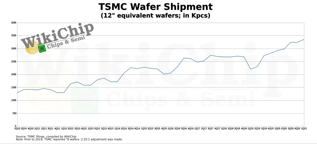
In the first quarter of 2021, TSMC increased its wafer shipment by 3.36% to 3.359 million 12″-eq wafers. That’s an increase of 434,000 12″-eq wafers since the same period last year.
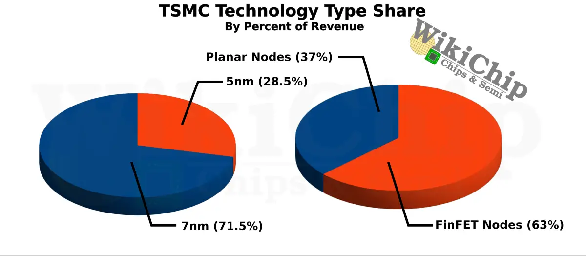
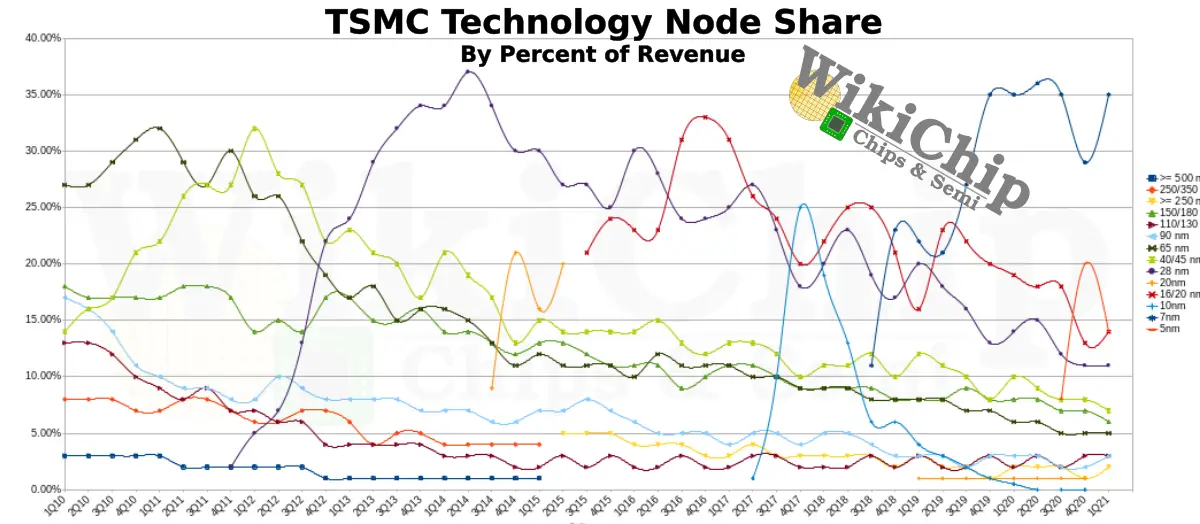
Interestingly, in their Q1 2021 earnings, TSMC redefined its “advanced technologies” term for the first time in almost half a decade. Previously the term referred to all FinFET-based technologies (i.e., 16 nm, 10 nm, 7 nm, and 5 nm). Now, TSMC redefined it to mean “7-nanometer and below”. In other words, they no longer consider 16-nanometer chips to be in the advanced technologies category. To that end, advanced technologies now account for 49% of total wafer revenue in the first quarter with 7-nanometer accounting for 71.5% of that portion. In total, FinFET makes up 63% of all wafer revenue.
On its own, 5 nm accounts for 14% of total wafer revenue, down from 20% last quarter. 7 nm accounts for 35% while 16nm is at 14%. Both 10-nanometer and 20-nanometer account for 0% of revenue which means everyone who was using those nodes migrated to either 16-nanometer or 7/5. All other legacy nodes remain flat quarter-over-quarter in terms of the share of the revenue. In terms of platforms, smartphones saw a decrease of 11%, making up 45% of total revenue. Meanwhile, HPC increased by 14% to make up 35% of total revenue this quarter. Automotive had the biggest increase with a 31% increase in growth but its impact on revenue is rather small, making up just 4% of revenue.
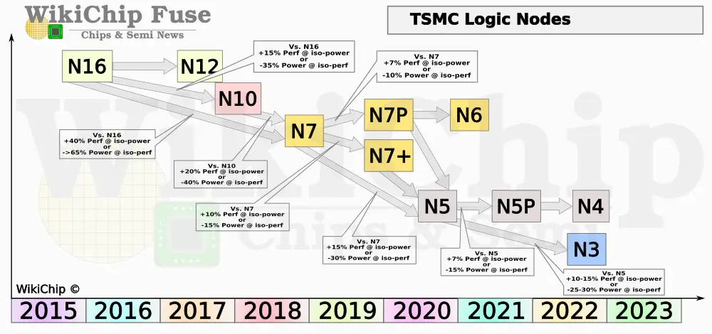
TSMC says it sees strong demand for its 5-nanometer node and expects revenue to reach 20% this year. The company also added an N4 node which is an extension of the 5-nanometer family. N4 offers a direct migration from N5 with compatible design rules while delivering better PPA. TSMC N4 is slated for risk production in the second half of this year with volume production planned for 2022.
The next full node stride from N5 is the N3 node. TSMC’s N3 will remain with FinFET devices as the company sees it as offering the best technology maturity, performance, and cost for the next node. Wei said “Our N3 technology development is on track with good progress. We continue to see a much higher level of customer engagement for both HPC and smartphone applications at N3 as compared with N5 and N7 at a similar stage.” Risk production for N3 is scheduled for this year with volume production expected for the second half of 2022. “Our 3-nanometer technology will be the most advanced foundry technology in both PPA and transistor technology, when it is introduced,” Wei added. TSMC expects N3 to be a long-lived node.
Samsung
This quarter Samsung announced it will doubling down on its foundry business. The company plans to invest 171 trillion won ($150.8 billion) in its development of cutting-edge process technology and the construction of new fabs (note the investment is exclusively non-memory related). The announcement is an increase of $50.8 billion from their prior “Vision 2030” announcement which was announced just a few months earlier. Last year Samsung announced its plans to boost capacity with a new EUV-based production line in Pyeongtaek, Korea. Construction started in June 2020. The new line, which is said to focus on their 5nm node, will enter volume production by the end of this year.
At their annual shareholder’s meeting, the company said it expects the ongoing chip supply/demand situation to cause a “slight problem” during its second quarter. In February, due to three severe winter storms, Texas suffered a major power outage. As a result, Samsung was forced to shut down its facility. Several other fabs by NXP and Infineon were also affected further straining the automotive chip supply chain. No production damage was sustained, but rather actual chip production was halted. Samsung’s Austin Fab produces 14nm, 11nm, and some trailing-edge processes. It’s believed that the facility accounts for as much as 5% of the global supply of 300m wafers and that the company suffered $100s of millions in production delays. Documents filed with the state of Texas in January revealed Samsung was looking to build a new $17 billion fab across from its existing Austin fab. It’s unclear if those plans were affected by the recent power crisis.
At a recent partner conference, Samsung reaffirmed their 3nm GAA node for 2022. The company is also introducing several new enhanced 10nm, 7nm, and 4nm nodes called 8LPA, 5LPP, and 4LPP. The new nodes offer a modest power and performance or power and density improvement over their predecessor while maintaining design rules and IP compatibility.
SMIC
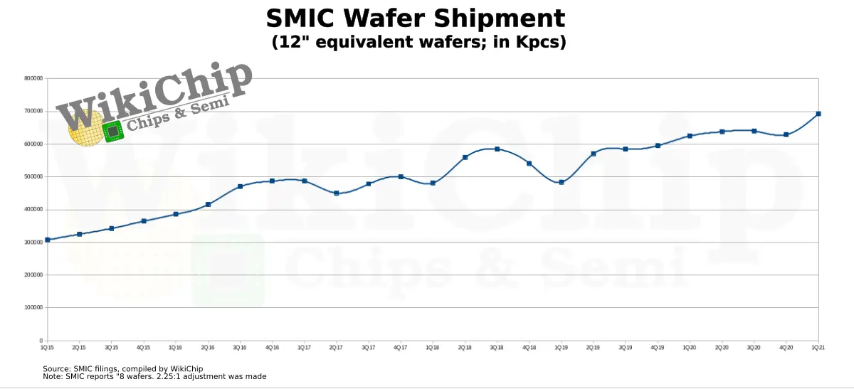
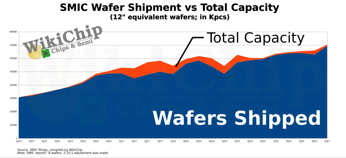
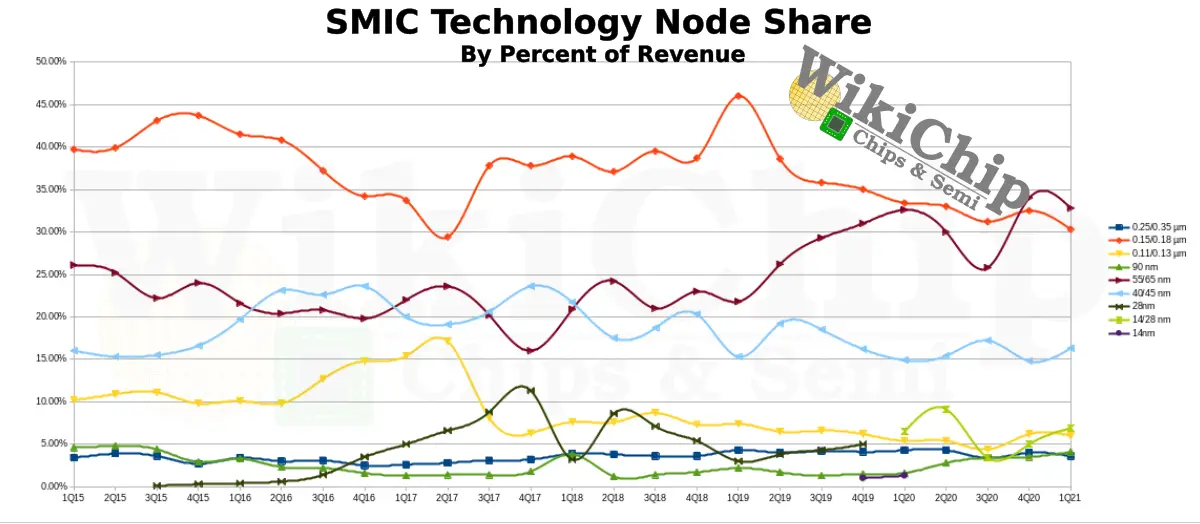
At SMIC, China’s largest foundry, spending was quite restrained. The company’s 2021 capital expenditures are approximately $4.3 billion, $1.4 billion lower than the $5.7 billion they spent last year. Moreover, SMIC says the majority of this will go into non-FinFET capacity expansion. The company shipped nearly 700,000 wafers this quarter (12″-eq) which is the highest ever reported. However, capacity is tight with shipment reaching 98.7% of SMIC’s installed capacity.
SMIC ramped its first FinFET device-based process – 14 nm – in the fourth quarter of 2019. Ramping it has been costly and the company lacks a driving customer (e.g., TSMC has Apple). For that reason, 14-nanometer and 28-nanometer combined account for just 6.9% of total revenue. SMIC says their 14-nanometer FinFET “had entered the mature stage of mass production and the product yield has reached the industry standard.” While 14nm and 28nm combined account for just 6.9% of revenue, by comparison, the company’s mature 150/180-micron and 55/65nm alone account for 63.1% of revenue.
To make the situation worse, the company is at its absolute limit in terms of capacity. SMIC says it will continue to add more capacity throughout the year, however, it warns that “certain restrictions on the company supply chain caused by the U.S. entity list created a lot of uncertainties in operational continuity and further capacity building and brought higher requirements to operational planning and engineering management.”
Last year the United States added SMIC to its entity list. “The Entity List designation limits SMIC’s ability to acquire certain U.S. technology by requiring exporters, reexporters, and in-country transferors of such technology to apply for a license to sell to the company. Items uniquely required to produce semiconductors at advanced technology nodes 10 nanometers or below will be subject to a presumption of denial to prevent such key enabling technology from supporting China’s military modernization efforts.” The move severely disrupted SMIC effort in advancing its leading-edge technologies, further ramping more advanced nodes, and conducting research and development of advanced process technologies.
SMIC has been working on a second-generation FinFET process. The company has never publically shared any details of its 14-nanometer or that second-generation FinFET process, therefore it’s impossible to judge how well it compares to other foundries. SMIC says that “compared with the previous generation, the second generation FinFET technology has greatly improved the transistor density per unit area, completed the development of low voltage process, and enter risk production.”
–
Spotted an error? Help us fix it! Simply select the problematic text and press Ctrl+Enter to notify us.
–