
TSMC Announces 6-Nanometer Process
Last week TSMC provided an update on their 5-nanometer node which has entered risk production. Today, TSMC is unveiling the addition of a new 6-nanometer process.
6-nanometer
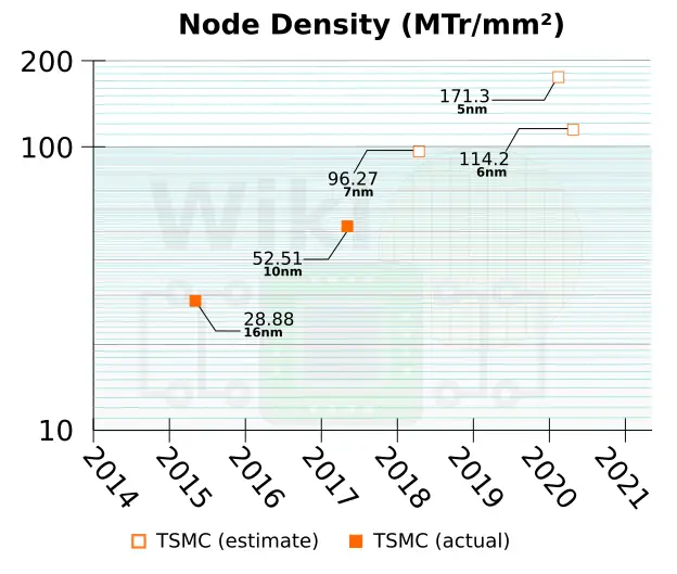
The new 6-nanometer node is said to leverage their new extreme ultraviolet (EUV) lithography expertise they have gained from their 7nm+ process technology which is currently in risk production. Compared to their normal (DUV) 7-nanometer node, TSMC is reporting an 18% higher logic density improvement while maintaining full design rule compatibility. Doing so offers a simple and straightforward migration path for customers looking for better PPA with limited resources. In other words, 6nm appears to be a cost-sensitive optimized derivative of their 7nm node. By our estimates, TSMC 6-nanometer node has a density of 114.2 MTr/mm².
| Estimated Design Rules For 6 nm | |||
|---|---|---|---|
| 7 nm | 6 nm | 5 nm | |
| CPP | 54 nm | 54 nm | 48 nm |
| MMP | 40 nm | 40 nm | 30 nm |
| Density | 96.27 MTr/mm² | 114.2 MTr/mm² | 171.3 MTr/mm² |
The details of the node remain vague for now. We expect to hear more about their roadmap at the upcoming TSMC Technology Symposium which will be held next week in Santa Clara.
TSMC expects 6-nanometer to enter risk production in the first quarter of next year.
–
Spotted an error? Help us fix it! Simply select the problematic text and press Ctrl+Enter to notify us.
–