
TSMC Talks 7nm, 5nm, Yield, And Next-Gen 5G And HPC Packaging
Following the conclusion of the 2019 VLSI Symposium in Japan, TSMC held a small press briefing. TSMC also delivered a packaging talk during SEMICON West 2019. This article is a summary of both events.
N7
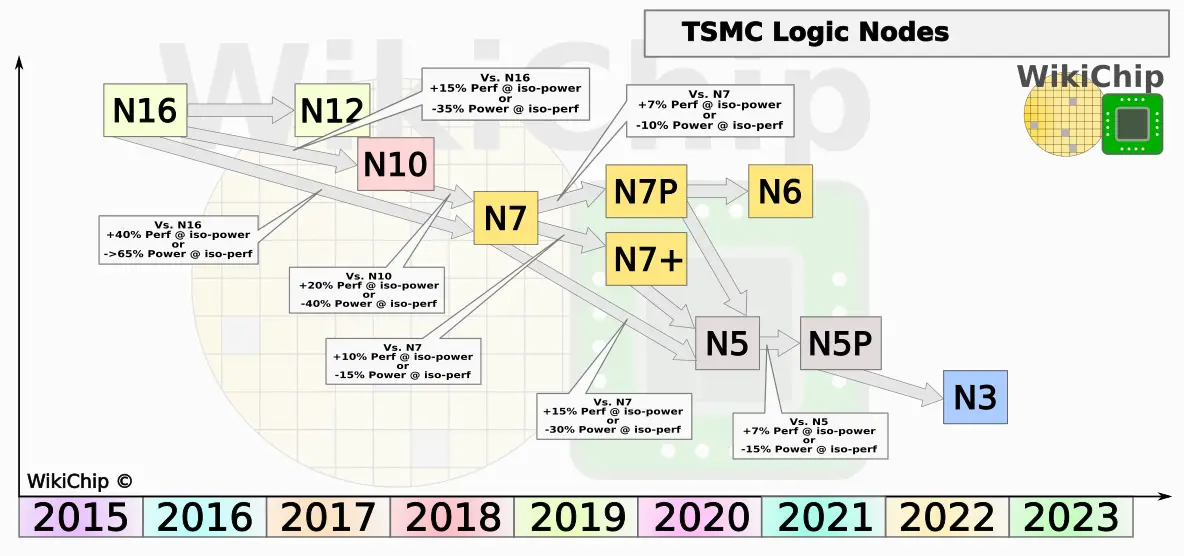
TSMC considers their 7-nanometer node (N7) the most advanced logic technology currently shipping. WikiChip generally agrees with this assertion. At the recent VLSI Symposium TSMC co-authored a paper on their 7-nanometer node which we have recently covered that goes into the design rules details. Other than a handful of key lead customers, most TSMC customers are said to go directly from their N16 to N7. Their N10 node is considered to be a short-lived node, largely intended to serve as yield-learning. When going from N16 to N7, N7 provides 3.3x routed gate density as well as around 35-40% speed improvement or 65% lower power.
| TSMC Node Comparison | ||||
|---|---|---|---|---|
| Node | 16 nm | 10 nm | 7 nm | 7nm/10nm Δ |
| Gate | 90 nm | 66 nm | 57 nm | 0.86x |
| Min Metal | 64 nm | 42 nm | 40 nm | 0.95x |
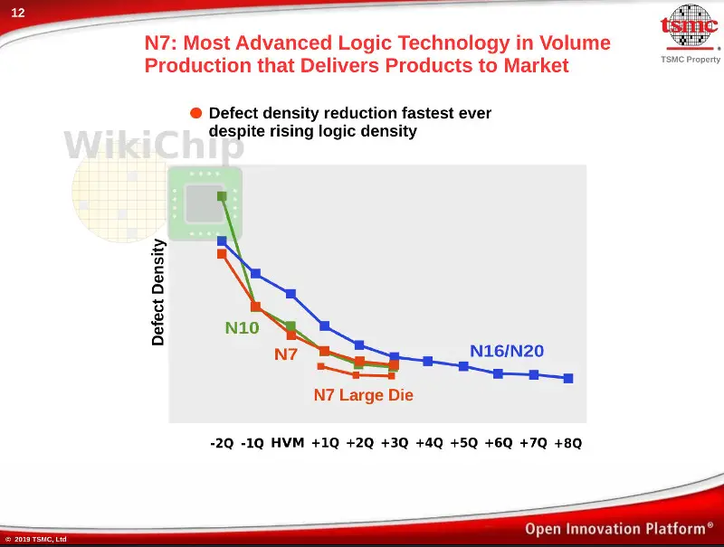
A key highlight of their N7 process is their defect density. TSMC says that learning from their N10 node, N7 D0 reduction ramp was the fastest ever, leveling off to comparable levels as the prior nodes. With the company pushing into HPC, they have started reporting defect densities separately for mobile customers and HPC customers with die sizes of 250 square millimeter dies and larger.
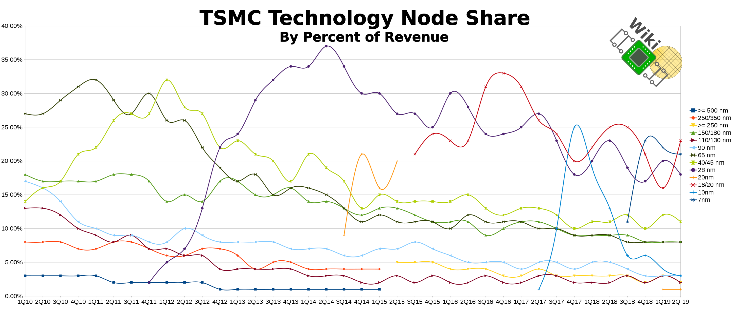
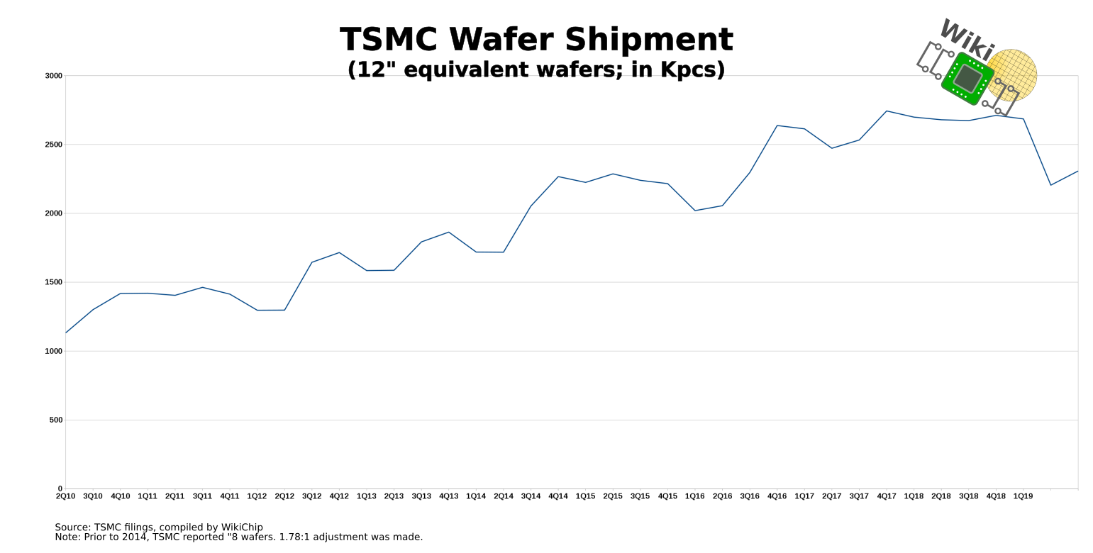
TSMC saw demand for their 7-nanometer node decreased slightly at around 1% quarter-over-quarter for the last half-year. The lion share of the revenue continues to come from their very mature 16-nanometer node. Q2 saw a slight increase in wafer shipment, however, that’s expected for a Q2 in general. When compared longer trend, this is actually the lowest volume for Q2 in 3 years. Nonetheless, they believe that N7 will reach 25% of revenue for the full year.
N7P
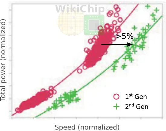
TSMC has started rolling out an optimized version of their N7 process called N7 Performance-enhanced version (N7P). This process goes by various other names such as “2nd generation 7 nm” and “7 nm year 2”. This process should not be confused with N7+. N7P is an optimized, DUV-based, process which uses the same design rules and is fully IP-compatible with N7. N7P introduces FEOL and MOL optimizations which are said to translate to either 7% performance improvement at iso-power or up to 10% lower power at iso-speed.
N7+
TSMC’s N7+ is their first process technology to adopt EUV for a few critical layers. N7+ entered mass production last quarter (Q2). TSMC says they have demonstrated similar yield to N7. Compared to their N7 process, N7+ is said to deliver around 1.2x density improvement. N7+ is said to deliver 10% higher performance at iso-power or, alternatively, up to 15% lower power at iso-performance. On paper, N7+ appears to be marginally better than N7P. Though keep in mind that those improvements can only be obtained through a new physical re-implementation and new EUV masks.
N6
N6 is the EUV equivalent of N7. It is planned to use more EUV layers than N7+. It is both design rule and IP-compatible with N7 and is intended to be the main migration path for most customers. N7 designs may be taped out again on N6 leveraging EUV masks and the fidelity improvements or re-implemented to take advantage of the poly over diffusion edge (PODE) and continuous diffusion (CNOD) standard cell abutment rules which are said to provide an additional 18% density improvement. It’s worth highlighting that N6 is unique in that it will actually enter risk production early next year and ramp by the end of the year 2020. This means it will ramp after N5. For that reason, TSMC says that N6 builds on both N7+ and N5 EUV learnings.
N5
TSMC 5-nanometer process is the next ‘full node’ after N7. N5 entered risk production in Q1 of this year and they expect the process to ramp in the first half of 2020. TSMC has said that a number of tapeouts are already underway. N5 uses EUV extensively on “many layers”. TSMC has demonstrated very high yield and has said they are on a similar trajectory, in terms of D0, as their N7 process. N5 is planned as a long-lived node and is expected to ramp, in terms of revenue, faster than N7.
Compared to N7, N5 is said to deliver 1.8x routed logic density. In terms of performance, N5 will have either 15% higher performance at iso-power or 30% lower power at iso-performance. Like N7, N5 will have two flavors – mobile customers and HPC. HPC cells will offer an additional option for up to 25% performance improvement over N7.
| Estimated Design Rules For 5 nm | |||
|---|---|---|---|
| 7 nm | 5 nm | ||
| CPP | 57 nm | 48 nm | |
| MMP | 40 nm | 30 nm | |
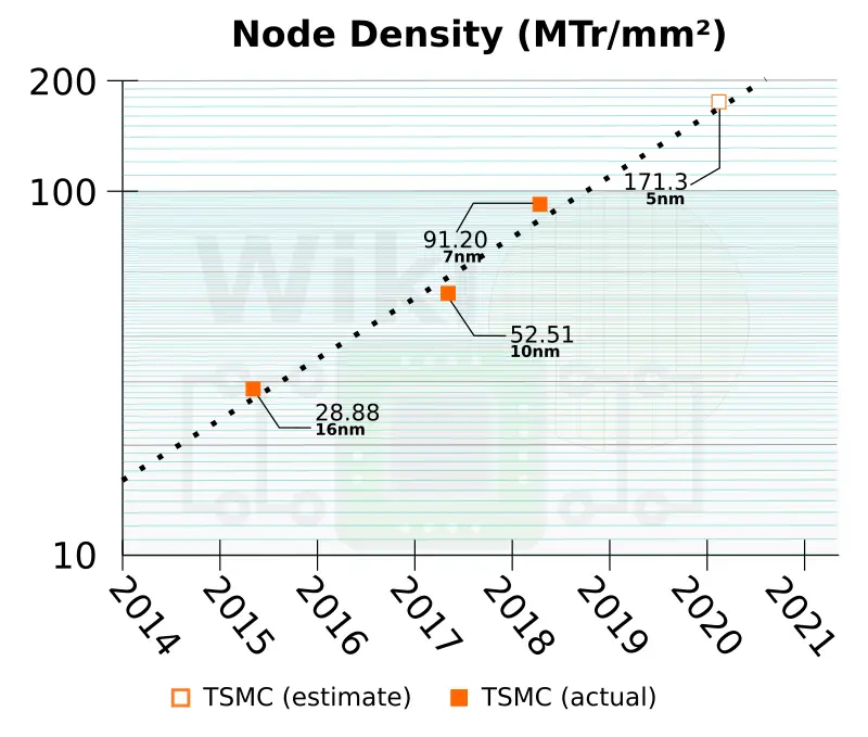
| Density | 91.2 MTr/mm² | 171.3 MTr/mm² | |
Ramping early next year, by our estimate TSMC will be a ‘full node’ ahead of both Intel and Samsung.
N5P
As with their 7-nanometer process, TSMC will offer an optimized version of their N5 process called N5 Performance-enhanced version (N5P). This process uses the same design rules and is fully IP-compatible with N5. Through FEOL and MOL optimizations, N5P will offer 7% higher performance over N5 at iso-power or 15% lower power at iso-performance. They are a little vaguer as to N5P timeline but they have hinted at sometimes by the end of 2020 or early 2021.
N3
TSMC has stated that their 3-nanometer process is going well. N3 is expected to be introduced around 2022. While TSMC has previously talked about GAA as a potential successor to FinFET, both TSMC and Intel have been making a case that FinFET, which is currently easier to manufacture, can be extended in performance sufficiently enough for another node. We currently believe that TSMC might be staying with FinFET for their N3 but will move over to GAA in a subsequent node.
–
Spotted an error? Help us fix it! Simply select the problematic text and press Ctrl+Enter to notify us.
–