
IEDM 2017: Sony’s 3-layer stacked CMOS image sensor technology
![]() While we don’t usually cover sensors as its out of our scope, we couldn’t pass on this one. At the at the 63rd IEEE International Electron Devices Meeting (IEDM), Sony presented the industry’s first 3-layer stacked state-of-the-art CMOS image sensor (CIS) technology. The technology shares many similarities with the research being done in the computing world.
While we don’t usually cover sensors as its out of our scope, we couldn’t pass on this one. At the at the 63rd IEEE International Electron Devices Meeting (IEDM), Sony presented the industry’s first 3-layer stacked state-of-the-art CMOS image sensor (CIS) technology. The technology shares many similarities with the research being done in the computing world.
Sony is no stranger to being first when it comes to die stacking. They were one of the earliest to adopt TSVs in high-volume manufacturing for their CIS chips in order to reduce the form factor. By taking the backside illuminated sensors and flipping it and thinning it, they could bond it directly onto the logic circuit with the use of TSVs as interconnects. At IEDM, Sony was back to present their 3-layer stacking technology which now included DRAM.
Rolling shutter distortion
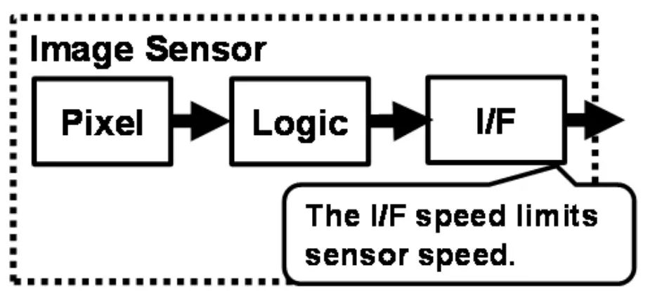
As smartphones and other mobile devices are continuously improving and are approaching digital still cameras, there are still a number of unresolved problems. One such problem is the interface speed. Conventional CMOS image sensor (CIS) chips collect the signal data from the pixels and send it through the logic circuit and out through the interface serially. This inherently restricts the CIS chip speed to the output speed of the interface which in turn means that the pixel reading speed is also capped at that speed. Because the reading speed can only be increased up to 30 fps, the difference in read time from the first pixel to the last results in the rolling shutter effect. For example, consider situations such as with moving objects in the picture. By the time the last pixel is read, the object may have moved some distance. This effect results in the object appearing to be swept back.
| Conventional CIS @ 30 fps | |
|---|---|
|

|
Temporary Buffer
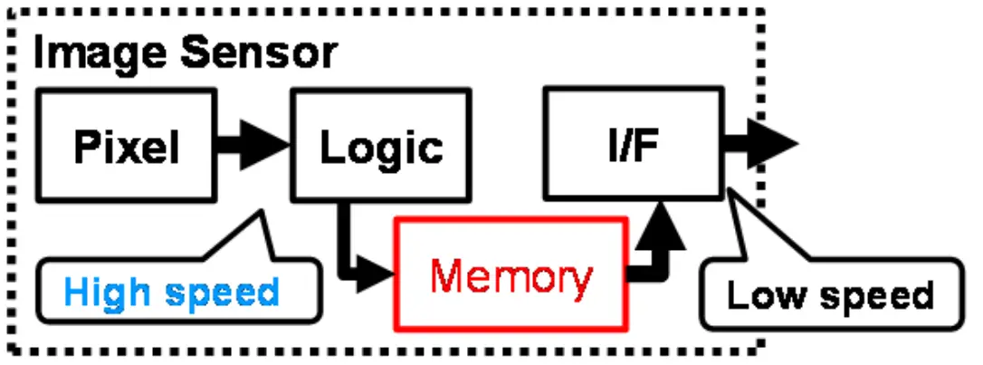
Previously, Sony has investigated a number of solutions such as using a structure with capacitance inside the pixel, however they have stated that those solutions cannot reliably scale as pixel size is reduced. Additionally, those solutions cannot be used for mobile applications such as a smartphone which greatly limits their usefulness. The new solution presented at IEDM is using DRAM to temporarily dump the pixel data onto, thereby decoupling the interface read speed from the pixel read speed. The CIS chip Sony developed had pixel reading speed increased by up to 120 fps.
| Sony’s CIS @ 120 fps | |
|---|---|
|

|
A Pixel/DRAM/logic 3-layer stacked CIS
The CIS chip presented consisted of 3 stacked dies. At the bottom is the 40nm logic substrate. On top of the logic die is the 30nm 1W DRAM which is placed like a flip-chip (i.e., facing downward at the logic). On top of the DRAM, at the very top is the 90nm backside illuminated (BI) pixels. The total thickness of the chip is reported at just 130 μm.
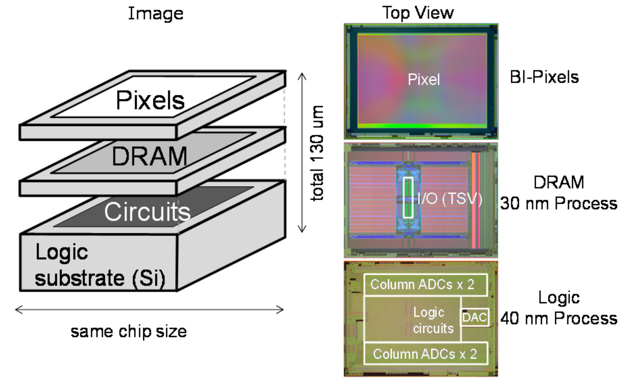
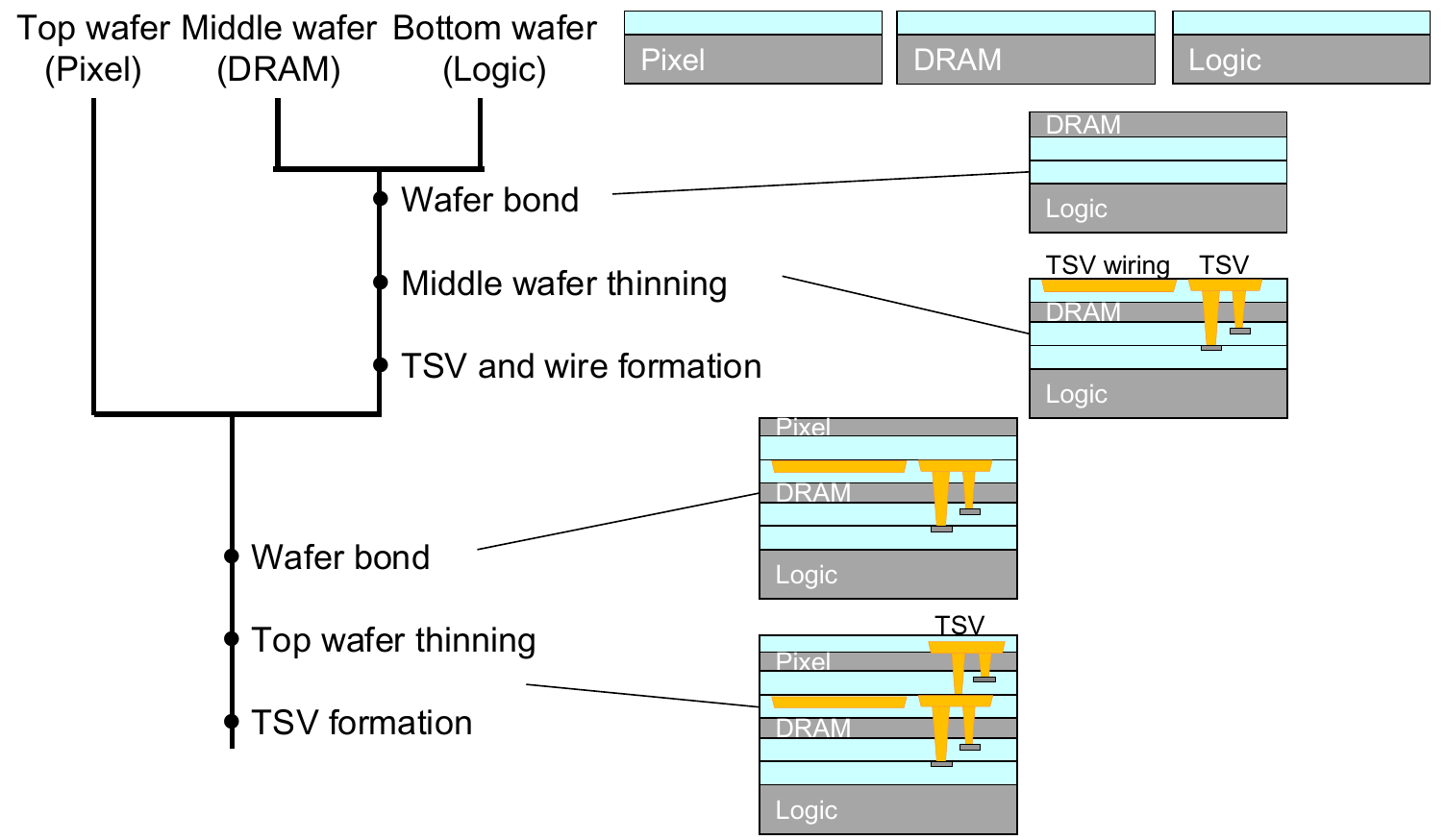
The logic substrate consists of 5 copper layers and 1 aluminum layer, the DRAM is 3 aluminum layers, and the BI pixels are 5 copper layers and 1 aluminum. Once the three wafers are fabricated, the DRAM wafer is flipped and is bonded face-to-face with the logic wafer (i.e., BEOL-BEOL). They then thin the DRAM wafer down to just 3 microns. Sony then forms the wiring and TSVs for connecting the two wafers. The 1 Al of the DRAM is connected to the top Al of the logic wafer. Note that Sony also uses those TSVs for the power and ground rails in order to simplify the circuit layouts.
Once that’s done, they then flips the pixel wafer and bond it to the DRAM/logic stacked wafer. As with the DRAM, they thin the backside of the pixel wafer and then form the TSVs. Like the DRAM-logic TSVs, the 1 Al of the pixel wafer is then connected to the Al of the DRAM wafer.
By placing the DRAM in the middle, thinning it, and developing narrow-pitched TSVs, Sony was able to reduce the I/O area and power consumption. It’s interesting to note that in fact Sony was able to achieve the same thickness as conventional 2-layer pixel/logic CIS stacked chips using this flow. Sony reported on various tests they have conducted using a sample of 9000 units. They concluded that the characteristics of the 3-layer stacked solution satisfied their product specification.
Commercialized 3-Layer Stacked CIS
Below is the TEM cross-section image of their commercial product clearly showing the pixels on the top, DRAM substrate in the middle, and the logic substrate at the bottom. The dotted lines are the interface between the two dies (pixel/DRAM and DRAM/logc). On the left is the pixel area which also shows the TSV wiring for the power and ground rails located at the top of the DRAM substrate. On the right is the peripheral area which shows the two-stacked TSV connecting the pixels and the logic substrate.
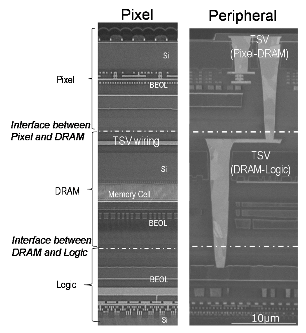
The final product is an impressive 19.3M pixels of 1.22 x 1.22 μm each and a 1 Gbit DRAM. Sony used TSVs that have a minimum diameter of 2.5 μm and a pitch of 6.3 μm with a line of 2 μm and space of 0.64 μm. In total they have over 35,000 TSVs – about 15,000 connecting the pixel substrate and the DRAM substrate and about 20,000 more connecting the DRAM substrate to the logic substrate.
The chip achieved 120 fps for all 19.3M pixels and can produce 960 fps FHD (1,920 x 1,080) super slow motion video.
Sony demonstrated the capabilities of the chip in this video which was also shown at IEDM.
–
Spotted an error? Help us fix it! Simply select the problematic text and press Ctrl+Enter to notify us.
–