
Hot Chips 30: Intel Kaby Lake G
Rumors of Intel using discrete AMD GPUs go back to at least late 2016. It wasn’t until last November that they officially announced it. What Intel came up with is their current generation of Thin and Light with High-Performance Graphics which went under the codename Kaby Lake-G. At Hot Chips 30, Srinivas Chennupaty, Senior Principal Engineer at Intel disclosed some of the motivation and technologies that went into designing those parts.
Motivation
Intel already makes mobile CPUs with integrated graphics with a decent baseline performance. What they wanted to do is take it a step further and satisfy the needs of high-performance graphics applications. At the time, and still is today with Intel’s H-series, the common solution was to bring an external mobile graphics processor. Those solutions work but they suffer from lower battery life and usually require a larger form-factor. The extra GDDR5 packages required also impacts the board area and thus the form-factor of the device.
The Package
The solution they came up with is to pack everything onto a multi-chip package. To keep the package size to minimum size, high-bandwidth memory was chosen over GDDR. At the time, this meant to be the first mobile part with HBM.
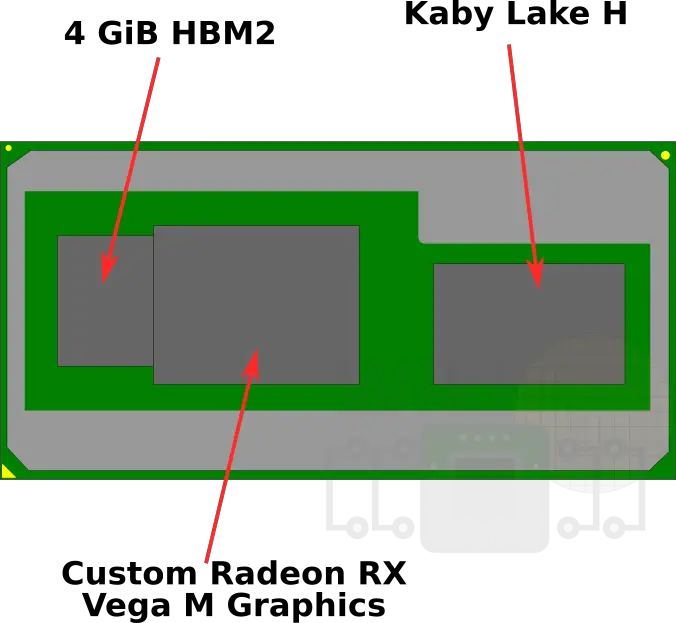
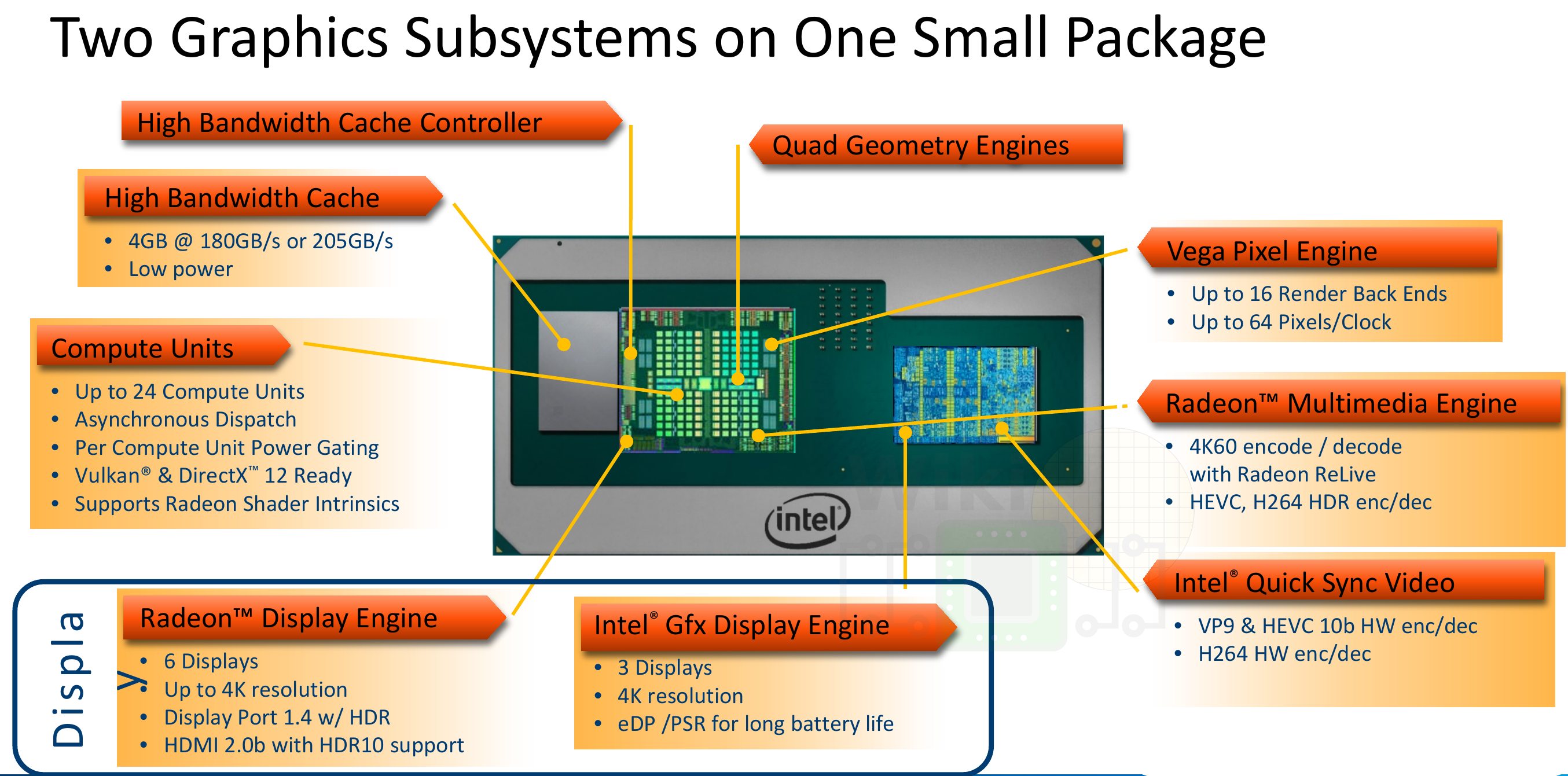
The package incorporates a Kaby Lake H processor, the AMD Radeon RX Vega M graphics, and the high bandwidth memory. The processor incorporates up to four cores and eight threads along with a Gen9.5 tier 2 integrated graphics meaning there are 24 execution units. The semi-custom Radeon RX Vega M comes with up to 24 compute units. Note that most of the specs were already discussed in detail before (see Kaby Lake G & Kaby Lake uArch).
By the way, with both the integrated graphics and the Radeon Vega GPU, this chip can support a total of nine displays (some devices such as their NUCs exposes them all).
Technological Convergence
Chennupaty explained that at around the same time (2015), two critical technologies that were used for Kaby Lake G neared completion. Though they were developed independently of this project, both were critical in the making of this chip. The first one was Intel’s embedded multi-die interconnect bridge (EMIB), a 2.5D packaging solution that offers interposer-like electrical characteristics without the cost of a full interposer. The second technology was an extension to Intel’s Dynamic Platform Thermal Framework (DPTF) that allows other SoCs to hook into Intel’s existing thermal management control.
EMIB
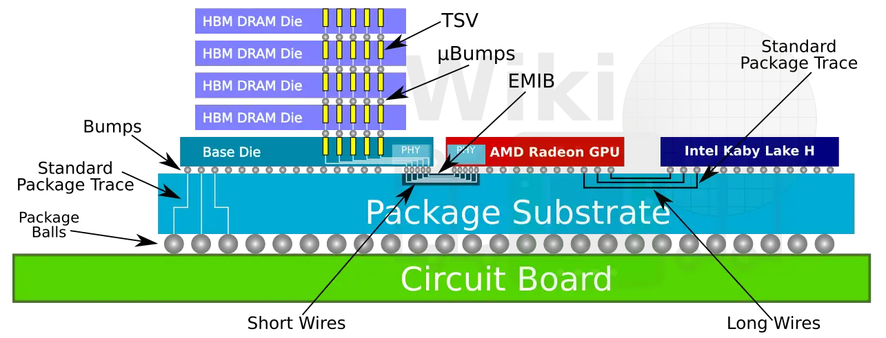
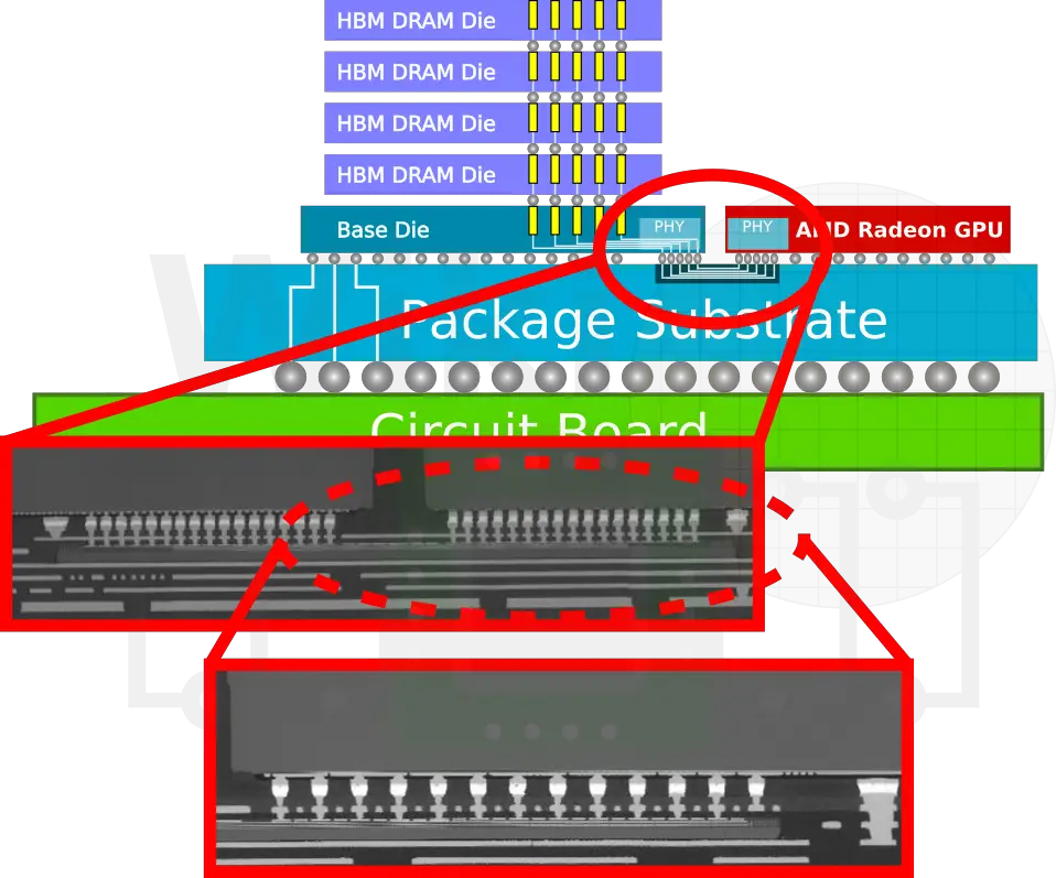
For Kaby Lake G, Intel decided to go with their EMIB technology. The reason is very simple. They needed an interconnect technology with good density for both die-to-die and die-to-package. An interposer, which is what AMD uses for their own GPUs, can do the job just fine. However, Intel has a slightly better technology which can use a much smaller silicon interposer embedded into the substrate. Like an interposer, an EMIB for this application is also ideal from a power envelop consideration where the EMIB short wires result in less energy transferring information between two PHYs compared to going through standard package traces. For Kaby Lake G, Intel uses an EMIB between the HBM and the Radeon GPU.
The high-bandwidth memory interfaces with the GPU using a 1,024-bit interface. Though there are a couple of different versions, they either use a 700 MHz clock (GL) or an 800 MHz (GH) clock for a total bandwidth of 179.2 GB/s or 204.8 GB/s respectively.
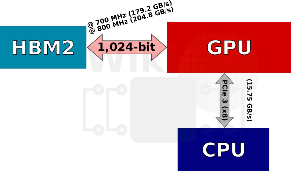
Note that the connection between the Intel processor and the GPU does not use an EMIB and instead uses the standard package traces. Chennupaty explained that while they were allowed to use any of Intel’s SoCs for this, they could not drive any changes to them. In other words, they had to use existing known good dies. This meant the connection to the GPU was restricted to the existing PCIe interface. Inherently this meant an EMIB is not really necessary. In theory, replacing the PCIe interface with a custom low-power solution (e.g., Intel’s Advanced Interface Bus) would have been much more fruitful but such modifications were simply out of scope. Furthermore, large changes to the silicon would have negated the quick TTM they were after. Using the standard PCIe interface within the package is not without its own set of challenges. While ordinarily the PCI express connection is designed for around eight to ten inches, in the case of Kaby Lake G those traces are less than two inches and do not leave the package substrate. Extra simulations and verification were necessary to ensure this kind of design would work as desired.
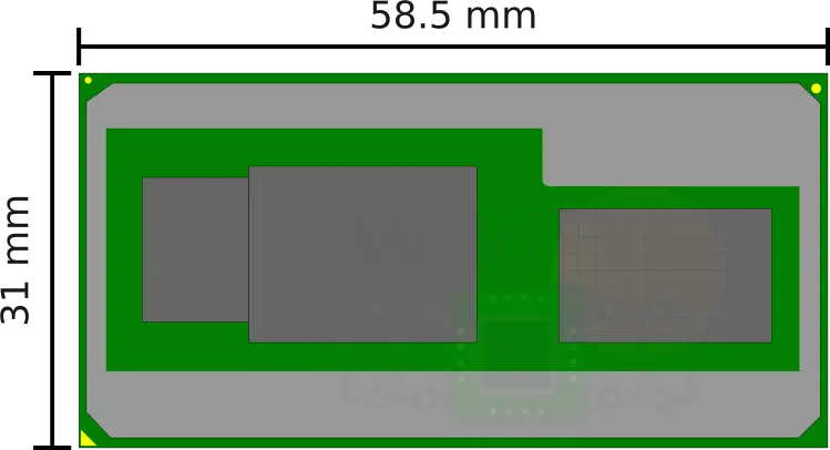
Because of the mobile form-factor, the chip is designed for, the components on the package have to be around the same height as the package stiffener that goes around the parameter of the chip which has a height of 1.7 mm. This was a problem because the HBM which was assembled at Micron ended up being taller than the rest of the components. To address this, Intel had to custom-thinned the HBM dies further to reach the required height. The whole process involves a complex supply chain from across three geographical areas from the fab to assembly.

Earlier we mentioned that the Radeon RX Vega M is semi-custom. Originally, AMD designed this product to use HBM with their interposer technology. Intel using it with their own EMIB technology meant the bump pitch was no longer compatible.
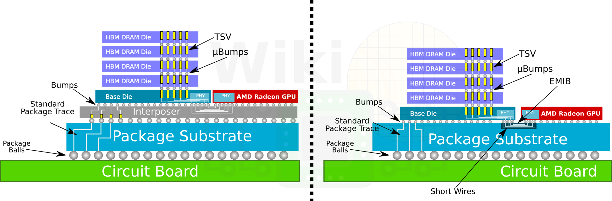
The geometry of the bumps had to be changed for Kaby Lake G to be used with Intel packaging technology.
–
Spotted an error? Help us fix it! Simply select the problematic text and press Ctrl+Enter to notify us.
–