
VLSI 2018: Samsung’s 2nd Gen 7nm, EUV Goes HVM
 For as long as anyone can remember, EUV has been “just a few years away.” This changed back in 2016 when Samsung put their foot down, announcing that their 8nm node will be the last DUV-based process technology. All nodes moving forward will use EUV. As Yan Borodovsky said at the 2018 SPIE conference, EUV is no longer a question of if or when but how well. At the 2018 Symposia on VLSI Technology and Circuits, Samsung gave us a first glimpse of what their 7nm EUV process looks like. Samsung’s second-generation 7nm process technology was presented by WonCheol Jeong, Principal Research Engineer at Samsung.
2nd Generation 7nm?
What Samsung presented at the symposia was what they consider “2nd generation 7nm”. Samsung naming is confusing and almost-intentionally obfuscated. I have asked Jeong about this and he said that by 2nd generation, they are referring to Samsung’s “7LPP” whereas their 1st generation refers to “7LPE” which will likely never see the light of day. Unfortunately, WikiChip has been through this situation before with Samsung’s presentation of their “2nd generation 10nm” last year which ended up being 8nm “8LPP”, therefore it’s entirely possible that this 2 gen 7nm node really refers to their “6nm” or “5nm” nodes. To avoid possible confusion, we will not be using “7LPP” and, instead, stick to the name Samsung used in their presentation (“2nd Gen 7nm”).
Design Features
Samsung’s second-generation 7nm process builds on many of their earlier technologies developed over the years.
- 5th generation FinFET
- 2nd generation hybrid N/P
- 5th generation S/D engineering
- 3rd generation gate stack
What’s interesting is that both their 2nd generation 7nm and their 8nm 8LPP share much of those rules including the fin, SD, and gate engineering. In fact, we can show the overlap much better in a table below which includes their 14, 10, 8, and 7 nanometer nodes.
| Samsung Technology Comparison | |||||
|---|---|---|---|---|---|
| Technology | 14LPP | 10LPP | 1st Gen 7nm | 8LPP | 2nd Gen 7nm |
| Fin | 2nd Gen | 3rd Gen | 4th Gen | 5th Gen | |
| Gate | – | 1st Gen | 2nd Gen | 3rd Gen | |
| S/D Eng | 2nd Gen | 3rd Gen | 4th Gen | 5th Gen | |
| SDB | 1st Gen | 2nd Gen | – | 2nd Gen | 3rd Gen |
| Gate Stack | – | 1st Gen | 2nd Gen | 3rd Gen | |
From a technology point of view, 8LPP shares many of the device manufacturing details with 2nd Gen 7nm, more so than the first-generation 7nm.
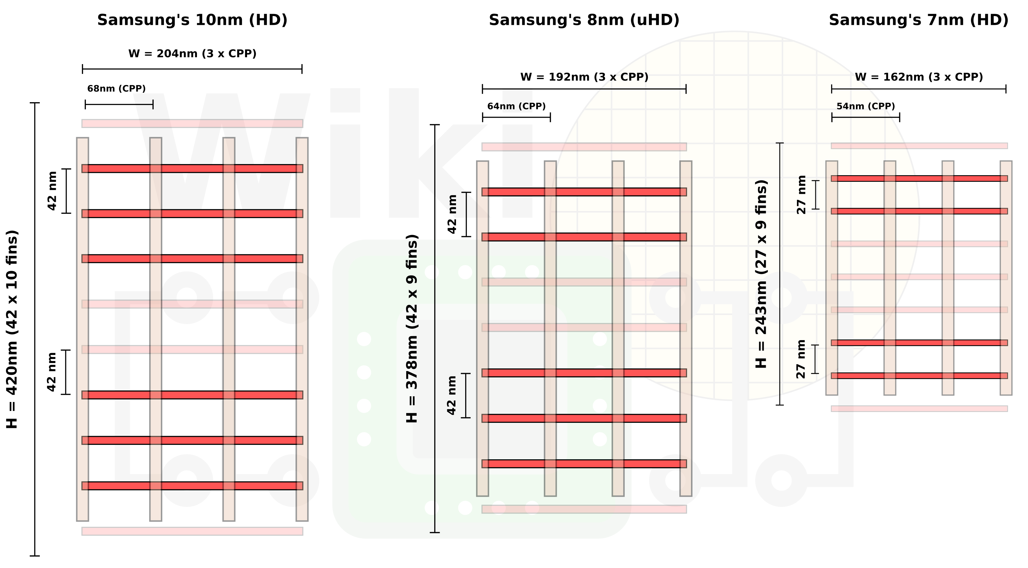
Key Dimensions
Samsung’s 7nm node key dimensions are:
| Samsung Technology Comparison | |||
|---|---|---|---|
| Feature | 7nm | 10 nm Δ | 14 nm Δ |
| Fin | 27 nm | 0.64x | 0.56x |
| Gate | 54 nm | 0.79x | 0.69x |
| M1, Mx | 36 nm | 0.75x | 0.56x |
All the pitches reported above are the tightest numbers reported to date for a leading edge foundry.
EUV
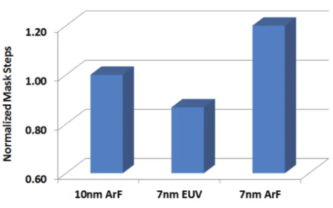
For their 10nm, Samsung has been using Litho-Etch-Litho-Etch-Litho-Etch (LELELE or LE3). For their 7nm, Samsung has eliminated most of the complex patterning by using a single-exposure EUV for the two critical layers. Note that for the fin, ArFi SAQP is being used. Samsung reports a mask reduction of >25% when compared to using ArF immersion lithography for comparable features which translates to cost and time reduction.
Cell
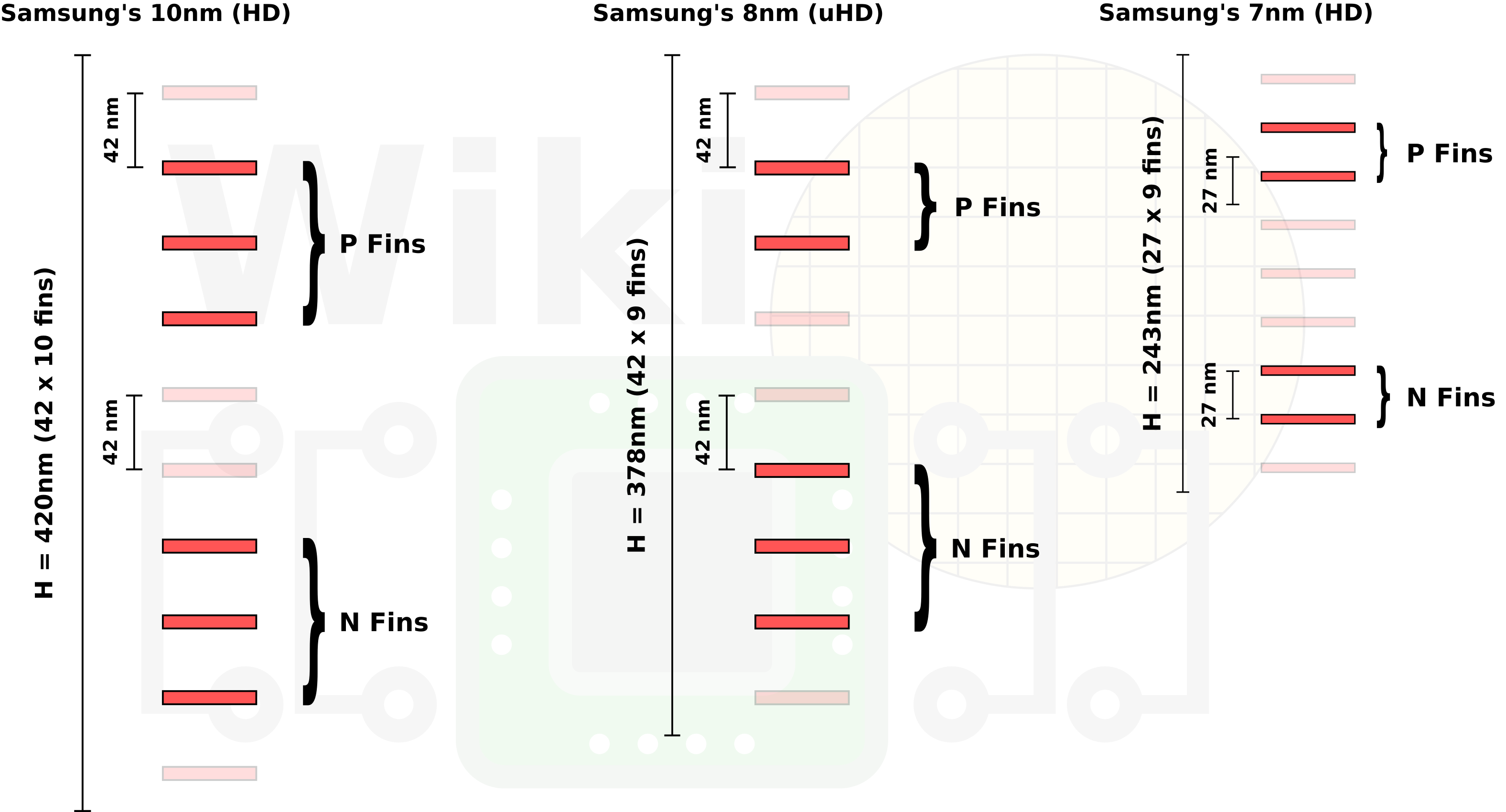
For their 7nm, Samsung’s high-density cell has a height of 9 fins or 243nm which works out to 6.75 tracks. This is a cell height reduction of 0.58x over their 10nm or 0.64x over their 8nm.
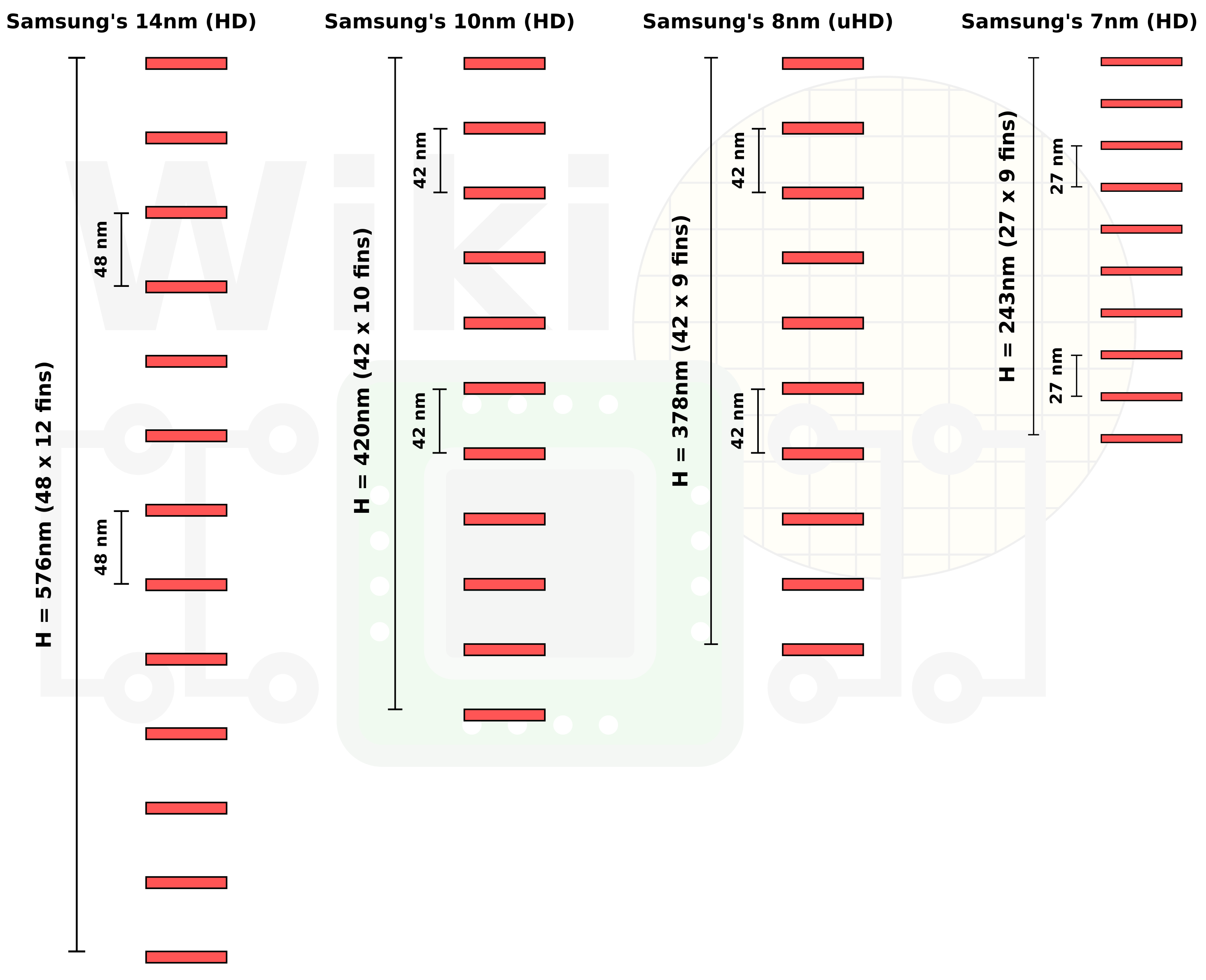
The high-density cell is a 2-fin device configuration.
For a NAND2 cell, 7nm take up a total area of 0.0394 µm², down from 0.0723 µm² in 8nm or 0.086 µm² in 10nm. That’s a 0.54x and 0.46x scaling for 8nm and 10nm respectively.
HP Cell
In addition to the high-density, Samsung also offers a high-performance cell.
| 2nd Generation 7nm Std Cell | ||
|---|---|---|
| Cell | HD | HP |
| Device | 2+2-fin | 3+3-fin |
| Height | 243nm 9-fin x 27nm |
270nm 10-fin x 27nm |
| Tracks | 6.75T | 7.5T |
–
Spotted an error? Help us fix it! Simply select the problematic text and press Ctrl+Enter to notify us.
–