
VLSI 2018: Samsung’s 2nd Gen 7nm, EUV Goes HVM
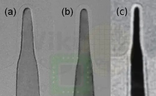
Fin Profile
Samsung improved the fin profile further. The usual improvements of making it taller, narrower and straighter were done. Samsung did not show what their 5th generation fins look like, but we have combined their 2nd (14LPP), 3rd (10LPP), and 4th (1st Gen 7nm) generation fins shown below as a, b, and c respectively.
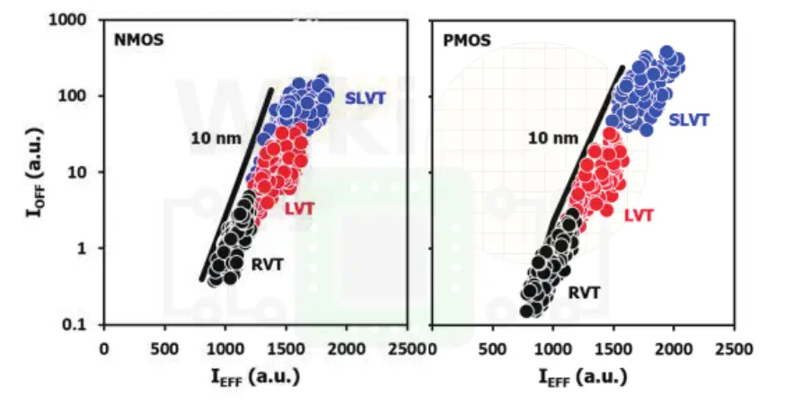
Power, Performance
So far, Samsung has presented around 5 papers on their 7nm process at various conferences and unfortunately, they have yet to provide good details of their device performance and power characteristics. A few more details were provided this time around. Compared to their 10nm technology and depending on the chosen library, for AC performance, Samsung is reporting between 30% and 50% lower power at a fixed frequency, or conversely, between 16% and 28% improvement in AC frequency at a fixed power.
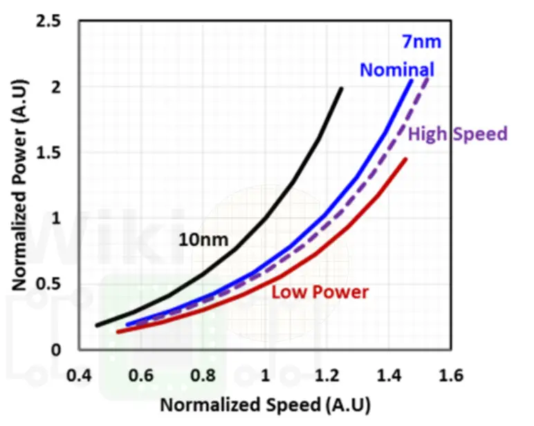
Samsung did not report the DC performance, but last year they compared their first-generation 7nm to 10nm. It’s unknown by how much 2nd generation has improved over the 1st generation, but compared to their 10nm, the DC performance improvements are very thin.
Readiness
The development of EUV spans decades and hundreds of billions of dollars in R&D. It’s not a surprise that industry is more than eager to recoup those costs. Samsung went all-in with EUV and in many ways, they are going to be lab rat everyone will be studying. Being first is risky but someone has to bite the bullet and get the ball rolling.
Perhaps the biggest question that remains is when will the process actually ramp? We got a different answer from just about everyone we asked – including among the Samsung engineers at VLSI! Officially Samsung expects to ramp 7nm late this year and through early next year. Unofficially we are told they are looking at late 2019 or even 2020 ramp. It’s worth noting that Samsung’s definition of ramp can be quite loose and can mean just some of their own products in lower volume; a definition that won’t fly with TSMC or Intel. Optimism for EUV was still fairly low among the conference attendees. Even Samsung does not project full confidence in their 7nm by introducing an 8nm process which shares many of the core technologies as their 7nm – offering marginal density and performance advantage. Moreover, back in 2016, Samsung told us EUV at 7nm was done, among many other reasons, in order to avoid quad patterning. Yet, they went ahead and designed an LE4 process just for their 8LPP anyway. Interestingly, both 7nm and 8nm are supposed to be ramping around the same time. It’s hard to not conclude that 8nm is, in fact, a backup plan, while their 7nm drags on.
Samsung didn’t really talk about yield during their presentation but they did demonstrate working SRAM shuttle dies with 256M bit SRAM arrays. For those dies, Samsung reported a wafer with around 50% yield. The dies appear to be near reticle size which usually has a maximum exposure field of 26mm x 33mm (858 square mm). This kind of yield at this stage for those kinds of dies is not a problem and doesn’t tell us much about the health of the process.
In addition to SRAM, Samsung demonstrated a fully working logic test chip which integrated a 6-core GPU along with a 4-core ARM CPU. No yield information was discussed for this chip.
What’s interesting is that Samsung is diving into EUV without all the pieces in place. For 7nm, significant work remains on photoresist in order to reduce defects to an acceptable level. Proper mask inspection tools are also not ready.
For their 7nm, there will be no use of pellicles initially which seems like something that should be a big deal for foundry customers. The rationale is that current pellicles with relatively low transmissivity (70s%) coupled with current power source levels (250W) are not good enough for high-volume manufacturing. While key industry players (ASML) insist that pellicles are not a showstopper, others (Dr. Turkot, Intel) argue that it’s a bigger issue. It’s worth pointing out that other foundries, such as GlobalFoundries’s 7nm, will also be introducing EUV without pellicles for this exact reason. However, unlike Samsung, GlobalFoundries is taking a much more conservative approach, initially only using it to reduce patterning for the contacts and vias layer. TSMC will also be introducing a lower capacity EUV variant next year.
While it’s unclear that EUV is 100% production-ready just yet, Samsung has taken the first step to bring it closer to mass production. It’s a move that someone has to make and one that the entire industry will be watching very closely as it progresses. EUV is a result of decades and hundreds of billions of dollars in R&D which will provide the industry with a way to prolong Moore’s Law.
Update: Our original story erroneously reported that EUV was being used for the fin. This was incorrect. Arfi SAQP is still being used for the fin. This article has since been corrected. We apologize for the mistake.
–
Spotted an error? Help us fix it! Simply select the problematic text and press Ctrl+Enter to notify us.
–