
VLSI 2018: Samsung’s 2nd Gen 7nm, EUV Goes HVM
Going EUV
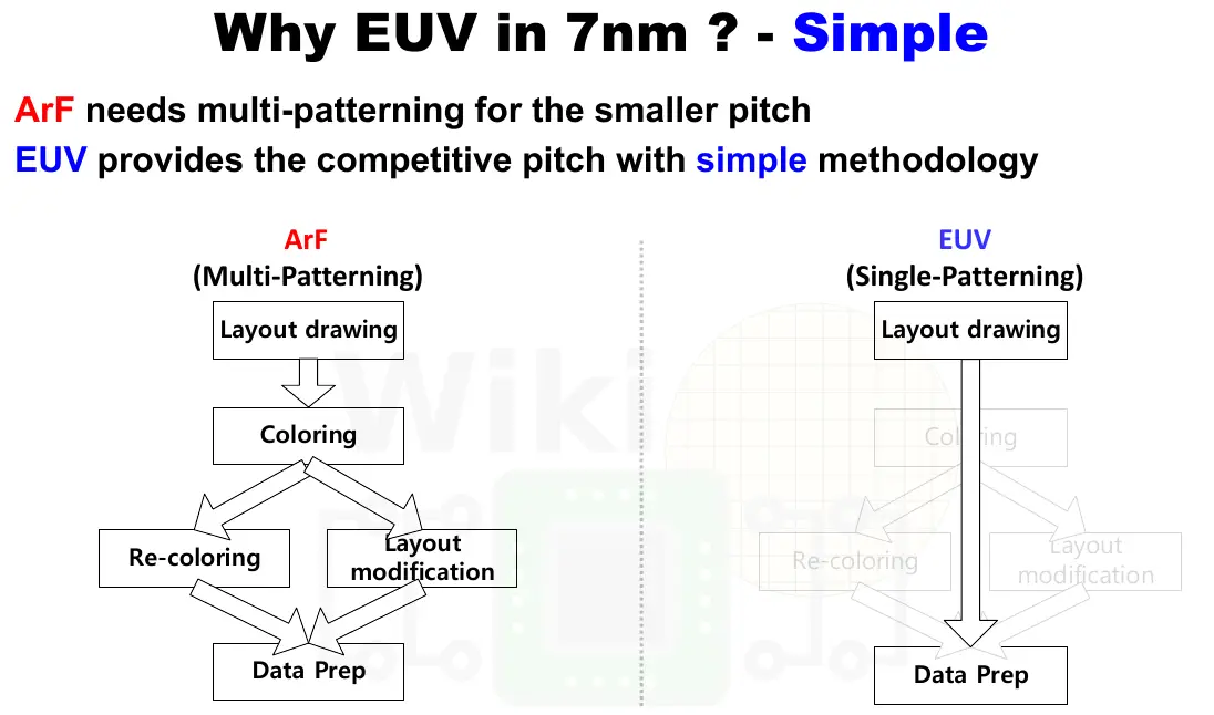
Samsung’s 7nm is an EUV-based process that takes full advantage of EUV lithography for their design rules. Samsung’s decision to go with EUV is a result of many factors including EUV readiness, cost, multi-patterning complexity, fidelity, and pitch scaling.
Simplicity
At least for their 7nm, the pitches are just within the single-patterning limit. This allows them to eliminate much of the design complexity associated with patterning (such as many of the coloring steps, a particular area that has been giving some manufacturers a very hard time).
Pattern Fidelity
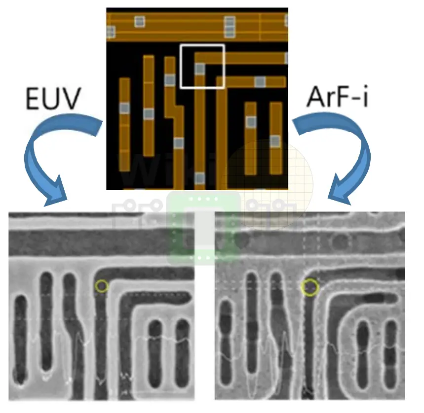
One of the many limitations with conventional multi-patterning techniques is pattern fidelity. What you see is often not what you get.
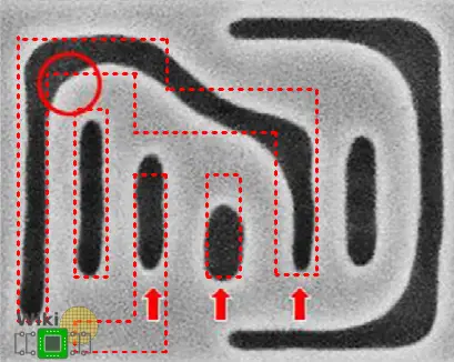
For their 7nm, Samsung is reporting EUV 2D fidelity to be 70% better than ArF multi-patterning.
Design Flexibility
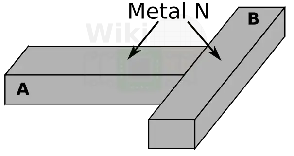
Samsung chose their design rules to allow for bi-directional metal routing under EUV. This provides them with some nice additional flexibility as far as VIAs go. For many recent process technologies, designers were limited, under MPT ArF, to uni-directional designs. This means that to get from one wire to the next we’d have to climb up to next layer and go back down to the next wire. In the cartoon example shown below, to connect A to B, we’d have to connect A-via-C-via-B.

By moving to EUV, routing gets simplified. In many cases, Samsung can eliminate the vias entirely such as in the example above which can become,
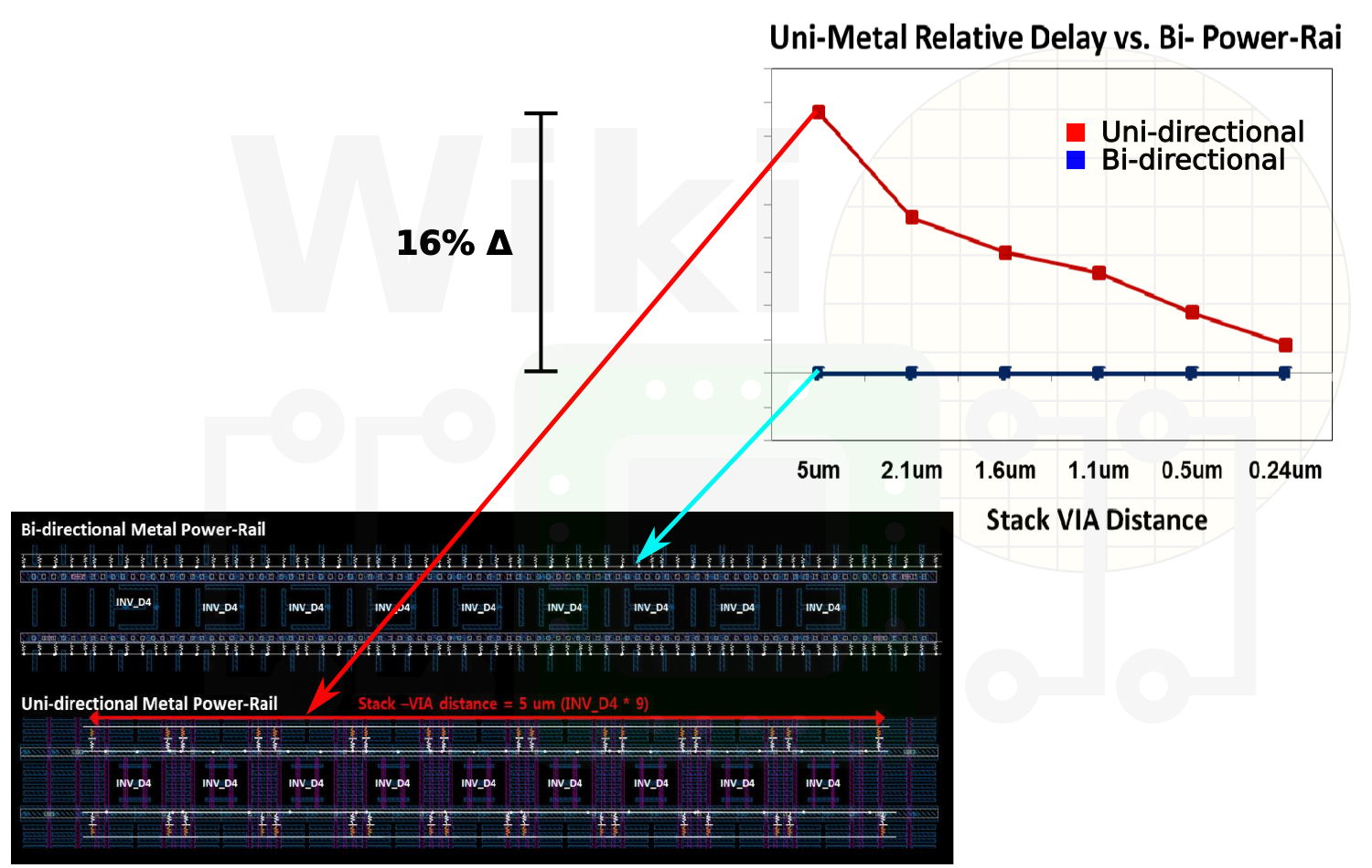
Conversely, more VIAs can be added when desired. This extra flexibility shows up in their power routing, providing additional VIAs with less IR-drop where wanted.
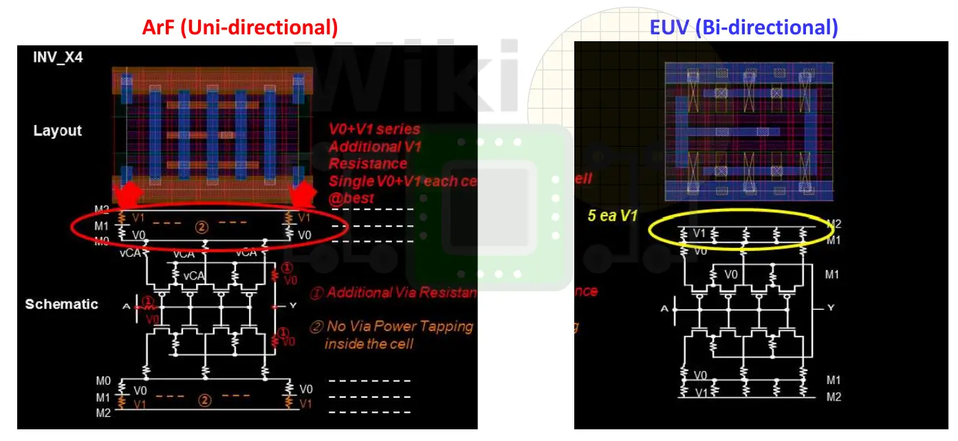
If we zoom in a little into that circuit, you can get a better idea of the resistance involved. For the conventional multi-patterning ArF uni-directional design, each cell gains an additional V1 resistance in series with the V0. Once they moved to a 2D design, this can be eliminated.
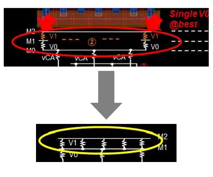
For their 7nm, Samsung says that the bi-directionality of the wires provides them with sufficient VIAs inside standard cells, this is in contrast to uni-directional designs which would be further limited by additional VIAs outside of the cell. To that end, Samsung reports up to 16% frequency improvement which gets directly impacted by the IR-drop of power-mesh over cell array. Note that this is for the best case of a simultaneous swing in a single power-rail.
Tighter CD distribution
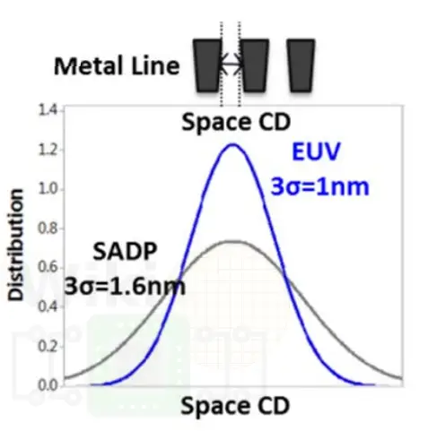
Shifting to EUV means a significant improvement in BEOL uniformity. Compared to ArF, EUV delivers a much tighten critical dimension (CD) distribution. Jeong reported space CD distribution improvement of 1.6x over SADP. The improvement in ADI CD distribution was even greater at over 2x improvement compared to ArF.
–
Spotted an error? Help us fix it! Simply select the problematic text and press Ctrl+Enter to notify us.
–