
AMD Announces Threadripper 2, Chiplets Aid Core Scaling
Yesterday, AMD announced the second-generation of their Threadripper family for the enthusiasts desktop market. The new models go up to 32 cores and 64 threads and will be available starting August 13.
Lineup
Four SKUs are being announced. All those processors are manufactured by GlobalFoundries on their 12nm FinFET process we recently detailed from the VLSI Symposium and are based on the Zen+ microarchitecture.
| 2nd-Generation Threadripper | ||||||||
|---|---|---|---|---|---|---|---|---|
| Model | C/T | Base/Turbo | L2 | L3 | TDP | PCIe | SEP | |
| 2990WX | 32/64 | 3.0 / 4.2 GHz | 16 MiB | 64 MiB | 250 W | 60 | $1,799 | |
| 2970WX | 24/48 | 3.0 / 4.2 GHz | 12 MiB | 64 MiB | 250 W | 60 | $1,299 | |
| 2950X | 16/32 | 3.5 / 4.4 GHz | 8 MiB | 32 MiB | 180 W | 60 | $899 | |
| 2920X | 12/24 | 3.5 / 4.3 GHz | 6 MiB | 32 MiB | 180 W | 60 | $649 | |
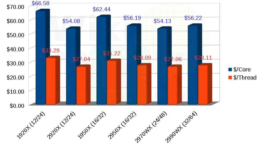
Going purely by the introductory price, second-generation Threadripper is now $12.50/core cheaper for the 12-core parts and $6.25/core cheaper for the 16-core model.
Features
For the most part, the SKUs are very similar to their first generation: they have four memory controllers for four channels and eight DIMMs and 64 PCIe lanes with 4 reserved for the chipset. AMD also bumped the supported JEDEC frequency to 2933 MT/s for a single DIMM per channels. All models received a modest frequency bump and have been upgraded to all the features that were introduced with Zen+ such as XFR 2 and Precision Boost 2.
Availability
The 32-core 2990WX will be available as early as August 13 with 2950X around August 31st. The 2970WX and 2920X won’t be available until October later this year.
More Chiplets to the Rescue
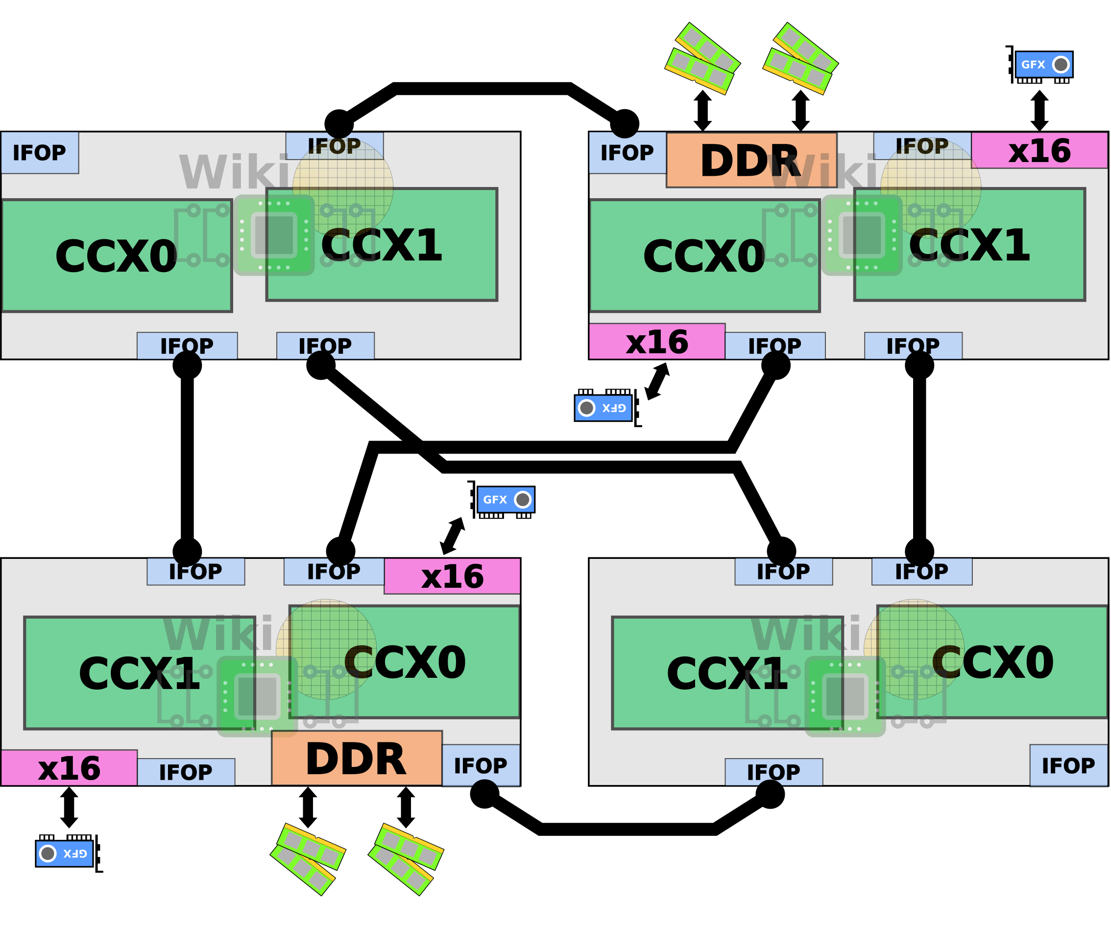
While the package configuration for 2920X/2950X is unchanged, the most interesting aspect of this launch is the introduction of 24- and 32-core parts.
Since a single Zeppelin incorporates only eight cores, to reach this core count AMD had to use four dies. But doing so means they have two memory controllers and 32 PCIe lanes per die with chip-level support for only four memory channels and 64 PCIe lanes in total. So how does that work?
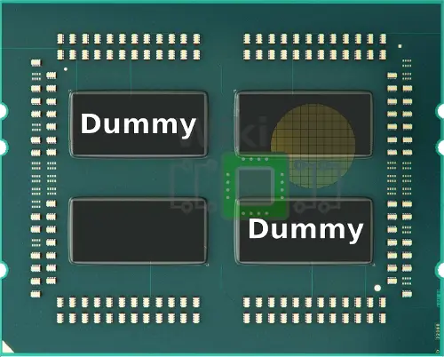
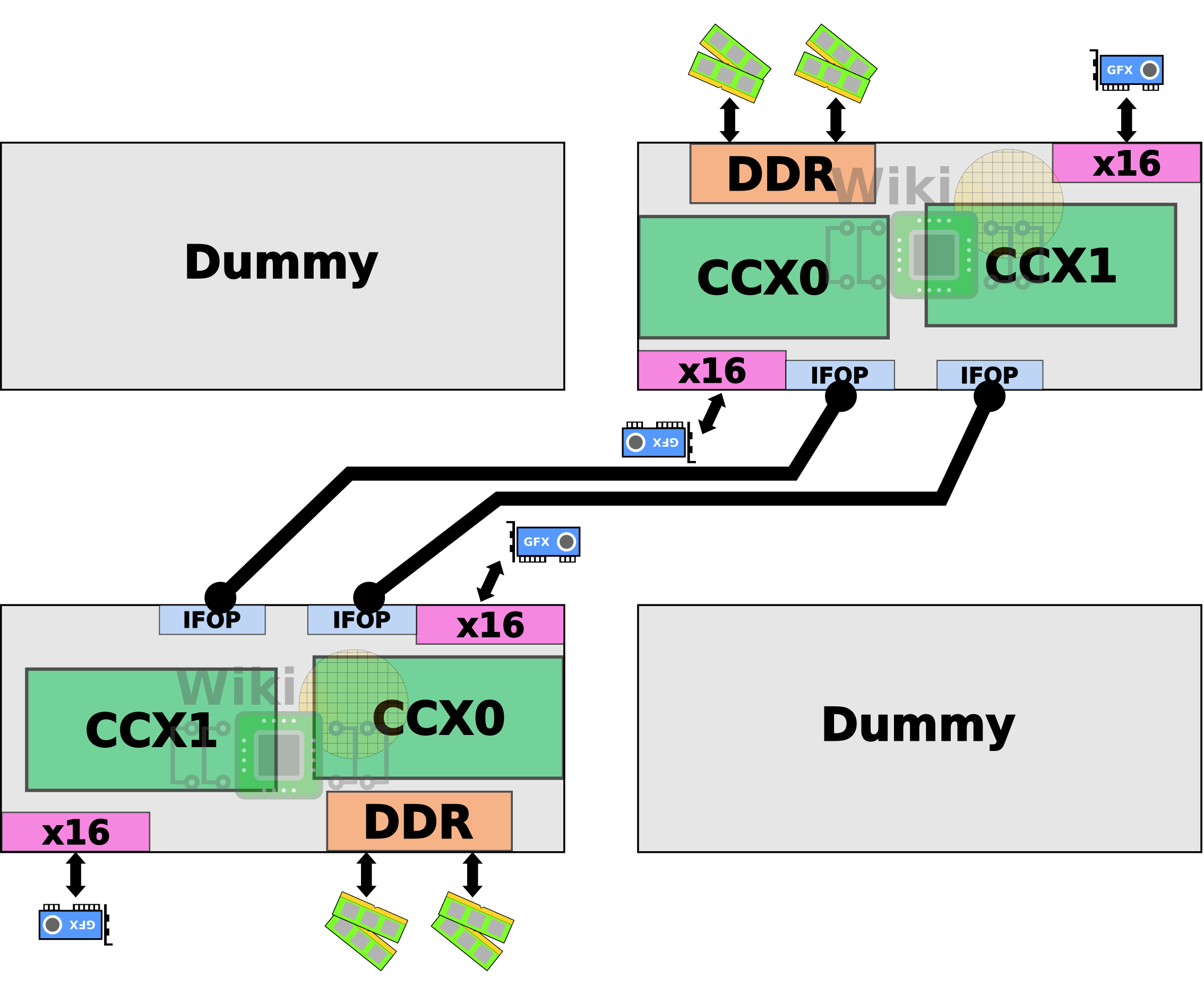
In the two-die configuration, the package contains two dummy dies for structural stability.
Those are wired via the AMD’s Infinity Fabric’s On-Package (IFOP) SerDes with two links per die.
Since AMD bumped the JEDEC specification support to 2933 MT/s (assuming no overclocking) from 2600 MT/s, at a MEMCLK of 1466.33 MHz, the total aggregated bandwidth between the two dies is increased from 85.33 GB/s to 93.85 GB/s. Note that for the press material provided to reviewers, AMD advertises a bandwidth of 102.4 GB/s (or 51.2 GB/s in one direction) which can only be achieved through overclocking the MEMCLK to 1600 MHz (DDR4-3200).
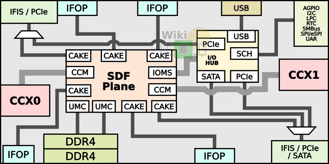
For the high core count chips, AMD introduced two new concepts: a compute die and an I/O die. A compute die is a Zeppelin without local I/O support. That is, a “compute die” has two CCXs and neither local DRAM access nor PCIe lanes. An I/O die is a full Zeppelin with the two CCXs, two memory channels, and 32 PCIe lanes. It’s worth noting that in practice, two dies are identical with the I/O subsystem just fused off but the semantics are important here.
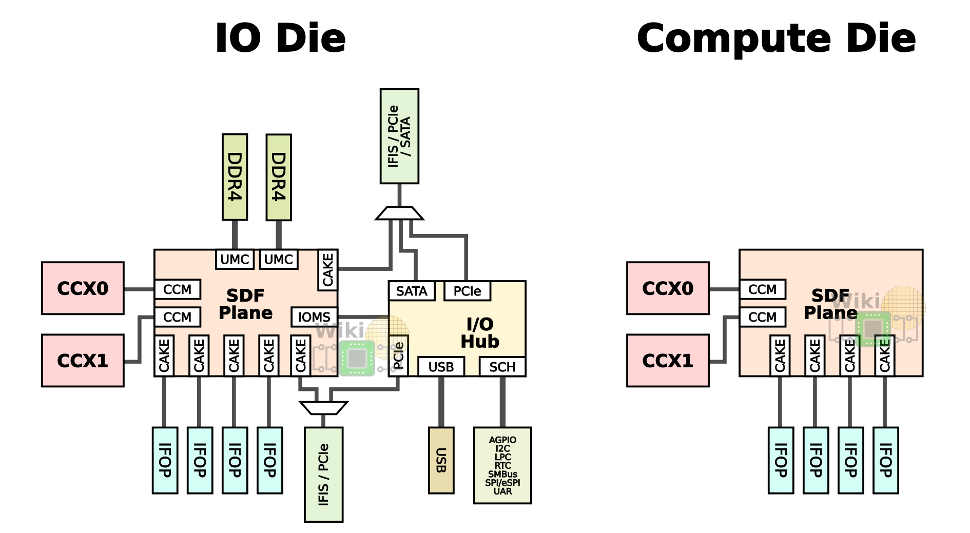
Instead of the dummy dies, AMD uses two “compute dies” in their place. This allows them to scale-up the core count without affecting the existing platform by changing the escape routing.
Like the dual-die configuration, bumping the MEMCLK to 1466.33 MHz bumps the link bandwidth from 42.67 GB/s to 46.92 GB/s and a bisectional bandwidth of 187.69 GB/s (17 GB/s higher from the 170.67 found in AMD’s EPYC parts). Note again that AMD advertises a bandwidth of 51.2 GB/s (or 25.6 GB/s in one direction) which is done through overclocking the MEMCLK to 1600 MHz (DDR4-3200).
Since two of the dies do not have local I/O and DRAM access, the cores must interface with the Cache-Coherent Masters (CCMs), through the CAKE module which encodes the request and sends it through the SerDes to a CAKE module on a remote die. The remote CAKE decodes the request and sends it to the appropriate UMC to the DRAM channel. The response is then routed back in the reverse order back to the request-originating core. To give you a sense of the latency involved, back at ISSCC, AMD reported around 145 nanoseconds round-trip for a system with a CPU frequency of 2.4 GHz and DDR4-2666 19-19-19 memory (i.e., MEMCLK of 1333 MHz).
It’s also worth noting that AMD offers a couple of operational modes, especially for gamers, that can disable and enable NUMA islands and affinitize memory accesses across their near region in order to improve performance for particular workloads. Nonetheless, in-depth benchmarking is required to fully understand the performance implications of this design.
–
Spotted an error? Help us fix it! Simply select the problematic text and press Ctrl+Enter to notify us.
–