
IEDM 2017: GlobalFoundries 7nm process; Cobalt, EUV
![]() We have known for a while now that GlobalFoundries was planning an aggressive shrink of their 14nm process. At the 63rd IEEE International Electron Devices Meeting (IEDM), GlobalFoundries presented their “late” paper on their 7nm process – “7nm Leading Performance” or “7LP” for short. The paper was presented by Dr. Premlatha Jagannathan. Jagannathan is responsible for the advanced technology materials engineering at GlobalFoundries.
We have known for a while now that GlobalFoundries was planning an aggressive shrink of their 14nm process. At the 63rd IEEE International Electron Devices Meeting (IEDM), GlobalFoundries presented their “late” paper on their 7nm process – “7nm Leading Performance” or “7LP” for short. The paper was presented by Dr. Premlatha Jagannathan. Jagannathan is responsible for the advanced technology materials engineering at GlobalFoundries.
The focus of the paper was about their 7nm CMOS technology platform for mobile and high-performance computing applications. The paper presented the work that was done by their 7nm development team.
Overview
We will start off with the laundry list of features and then dive into the specifics. The general attributes of this process are:
- Targets Mobile, SoC, HPC
- 2.8x routed logic density over their 14nm
- Provides 40% higher performance or 55% lower power over their 14nm
- Immersion lithography and advanced optical patterning (SADP, SAQP)
- Cobalt introduced for liner and the caps at the SAQP-critical layers
- EUV insertion plan in place, undefined timeline (i.e., “when ready”)
- Backbone of their next-generation ASIC services
- Complete set of foundation and complex IP available (e.g., core, peripherals, SerDes, Memories, 2 & 2.5D packaging)
14nm Reference Technology
Throughout the IEDM presentation, they made many comparisons against a 14nm reference node. This 14nm node was initially presented by Samsung at the 2014 IEEE International Solid-State Circuits Conference (ISSCC). Their 14nm node has been in production for over two years and has been used for a very diverse set of applications including high-performance computing, networks, and mobile application processors. A well-known example of such product is AMD’s Zen microarchitecture.
With that respect, their 7nm brings a full node density and performance scaling over the 14nm reference.
Key Dimensions
The key technology dimensions are shown below.
| GlobalFoundries 7nm Process | ||
|---|---|---|
| Feature | Pitch | Note |
| Fin | 30 nm | |
| Gate | 56 nm | |
| M0 | 40 nm | 1x |
| M1 | 56 nm | 1.4x |
| M2 | 40 nm | 1x |
| M3 | 40 nm | 1x |
As expected, GlobalFoundries is continuing with the use of a FinFET transistor. Their 7nm process features an aggressive fin pitch of just 30 nm which means Self-Aligned Quadruple Patterning (SAQP) will be utilized here. The gate pitch is at 56 nm. The 1x metal layers have a pitch of 40nm and are unidirectional. Like the gate patterning, the 1x metal layers will also make use of just Self-Aligned Dual Patterning (SADP). Note that three of the four layers listed are at 1x (M0, M2, and M3). M1 has a relaxed pitch of 56nm which is aligned with the gate.
As a side note, GF listed this technology as their third generation FinFET however 14nm was their first generation FinFET so we’re not exactly sure what they consider their second generation. It’s possible they refer to their 12nm as 2nd generation. However if that’s the case, apparently they did not seem to think it was important enough to list it on the roadmap they presented at IEDM which only listed 20nm, 14nm, and their 7nm.
Going After the Density
The aggressive scaling of design rules allowed GlobalFoundries to significantly scale of the standard cell. In their 14nm process, GlobalFoundries’ workhorse cell was a 9-tracks, four fin cell.
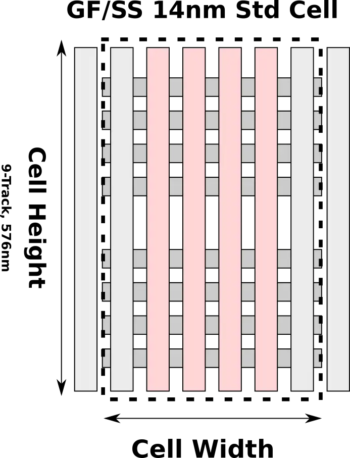
Having a metal pitch of 64 nm, this cell had the height of 576 nm.
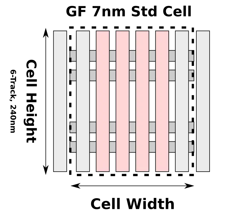
In their new 7nm process, the new workhorse cell is a 2-fin, 6-track cell. With a metal pitch of 40nm, the new cell has a cell height of just 240nm.
This very aggressive scaling which resulted in 0.42x in cell height reduction has an even larger impact at the SoC level. GlobalFoundries reports that the overall compaction compared to their 14nm reference is 0.36x at the SoC level (i.e., a mixture of various critical cells such as combinational gates, multi-input gates, complex cells, and flip-flops).
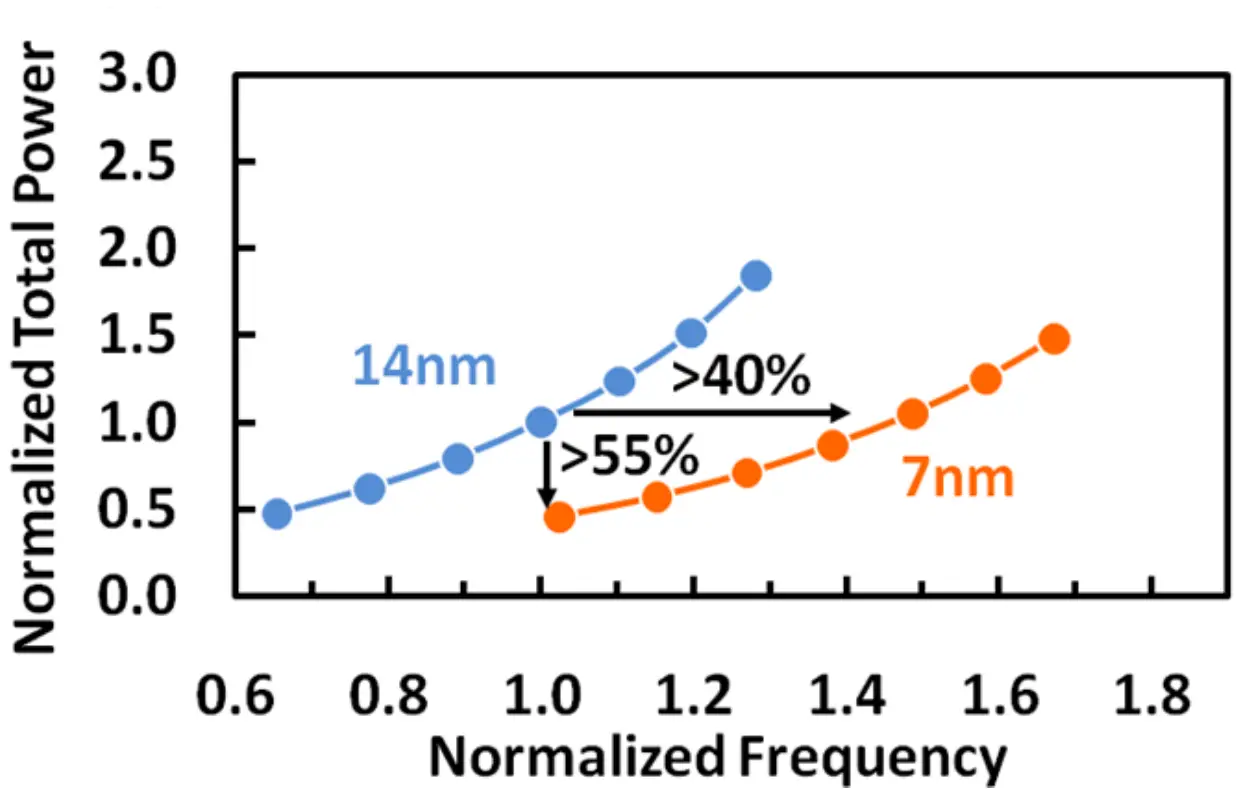
The graph above compares the power vs. the frequency of their 14nm reference node to their 7nm node. What can be seen is that for the same given power, there is 40% gain in performance. Alternatively, you can think of it as having >55% power reduction at a fixed frequency.
–
Spotted an error? Help us fix it! Simply select the problematic text and press Ctrl+Enter to notify us.
–