
IEDM 2017: GlobalFoundries 7nm process; Cobalt, EUV
EUV Insertion Plan
Jagannathan concluded his IEDM presentation by talking a little about GlobalFoundries strategy to inserting EUV into their 7nm HVM. The goal was to replace some of the multi-patterning techniques where aggressive pitches were used with EUV in such a way that no design update would be required to take advantage of this. Vias and contacts multi-patterning will be replaced with single exposure EUV.
GlobalFoundries claims this will lower the overall mask count of critical layers by 25%. It’s worth noting that the choice to limit EUV to only those constructs means GF adaptation of EUV will be very quick because no alteration to the design is needed. Unfortunately, it also means that there will be no density change or shrink of any kind. GF currently only has 1 EUV tool installed at their Fab 8 facility and is expected to introduce a second one by the end of this year or early next year.
There is no exact timeline for when GlobalFoundries is planning on inserting EUV but our general impression is that it will only be introduced “when it’s ready”.
GlobalFoundries is also planning a third enhanced version of this node where EUV will be used for more features. This will allow them to shrink some of the features and improve density, however it will also require designers to rework their designs to take advantage of this.
No Optimism For Pellicles?
It struck us as a little odd that GlobalFoundries limited their EUV insertion to contacts and vias so we searched around at IEDM for answers. EUV pellicles are transparent membranes that cover the mask during the production flow, keeping it clean. Being located away from the focal plane of the image means any particle that lands on the pellicle remains out of the focal plane. You can think of it as a dust cover preventing various unwanted particles (e.g., dust) from landing on the EUV mask and printing defects on the wafer. EUV pellicles are considered a requirement for high-volume manufacturing using EUV lithography. Due to their thin structure and fragility, EUV pellicle development progress has been extremely slow. However, we were told that it’s possible GlobalFoundries might be able to do without pillicles but only for the patterning of things such as vias and contacts which can explain why those are the only two things GF is planning to replace MP with EUV for their initial 7nm insertion.
Summary
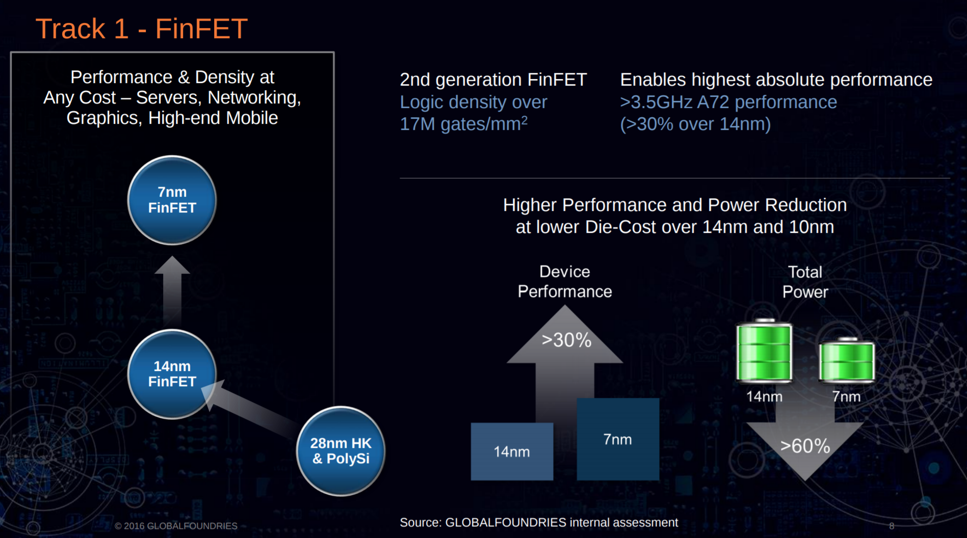
Overall, GlobalFoundries presented a very impressive 7nm process aimed at mobile and SoC as well as high performance through two sets of standard cells and two metallization stacks. The process features a 2.8x routed logic density over their 14nm with 40% higher performance (or equivalently, 50% lower power). Similarly they reported over 2x in density increase for their SRAM with complementary 2x increase in performance.
This process features a very aggressive fin pitch of 30nm which uses quad-patterning with a gate pitch of 56 nanometers which uses SADP. However, in order to maintain higher flexibility for their customers, GlobalFoundries restricted their BEOL to double patterning and a more relaxed metal pitch of 40nm. GlobalFoundries introduced for the first time cobalt into their process, but only for the liner and caps. Finally, GF introduced their (IBM’s) 2nd generation Multi-WF process which has been extended to cover the entire Vt range. This was done through the use of eight work-function materials covering four different threshold voltages.
Officially, GlobalFoundries is expected to introduce their 7nm in late 2018. Risk production is to begin in the first half of 2018 with PDK 1.0 available shortly after. Unfortunately we are not as optimistic and we think the real introduction will be around mid-2019 given some of the unsolved problems surrounding their process.
Some Math
We wanted to see where GF stands when compared to other leading edge foundries in terms of density.
| Leading Edge | |||
|---|---|---|---|
| Fab | GF (7nm) | Intel (10nm) | TSMC (7nm) |
| HP | 0.0353 µm² | 0.0441 µm² | |
| HD | 0.0269 µm² | 0.0312 µm² | 0.027 µm² |
| MTr/mm² | ~86 MTr/mm² (2F6T) | ~102.9 MTr/mm² | |
GlobalFoundries reported very dense 6T SRAM bit cells. For the SRAM bit cells, GlobalFoundry is actually over 15% denser and is somewhat similar to TSMC’s. We believe this large gap in density came from some performance related attributes that Intel simply could not sacrifice for their own products. In an ideal world, to really compare the two nodes we would take an open synthesizable core and fabricate it at each of the foundries. Unfortunately since that’s not really possible, we have to resort to less than ideal ways of comparing nodes. We have tried to apply Intel’s MTr/mm² equation to both GF and Intel’s to get some sort of a comparison. As a sanity check, Intel reports 100.8 MTr/mm² for their own process and GF reported 0.36x compaction vs their 14nm which works out to roughly our numbers. GF is around 86 MTr/mm² or roughly 15% lower density than Intel, despite having a shorter cell. Much of this is due to Intel’s innovative “hyperscaling” techniques which include the elimination of dummy gates at the cell boundaries, resulting in tighter packing of cells.
With all of this in mind, there is no clear winner here. Both technologies can certainly exchange punches. For chips that make use of large caches, GF can have a significant lead over Intel. Back in October Canard PC Hardware made the bold claim that AMD’s 7nm-based Zen 2 will feature 64 cores and a whopping 256 MiB of L3 cache (or 16 cores and 64 MiB of L3 per die if they still use quad-chiplets). For this kind of application, AMD will have significantly denser chips. However, Intel’s higher mix-logic density, superior local interconnects, and higher performance cells over GF 7nm 6-track cells do have their own distinctive advantages. GF did not detail anything about their own high-performance cells but we expect them to do very well and able to push IBM’s next generation z15 to at least 5 GHz to not regress in single-core performance.
Final Thoughts
A while back, when GlobalFoundries initially announced they had developed a 14nm process, they ended up really struggling with their first generation FinFET. In fact, things went so badly that they eventually gave up on their own process, ending up licensing Samsung’s 14nm process. What we are seeing today is a very different company with a very impressive leading-edge process they can offer to customers. It’s worth noting that a good chunk of the credit should be attributed to IBM whose patent portfolio and expertise GF acquired back in 2015 helped make this process a reality.
As impressive as the process is on paper, the real test is when they ramp-up production and start shipping 7nm chips in volume.
Update: We originally incorrectly reported that CPC Hardware stated Zen 2 will feature 128 MiB of L3 cache instead of 256 MiB. This has since been corrected.
–
Spotted an error? Help us fix it! Simply select the problematic text and press Ctrl+Enter to notify us.
–