
IEDM 2017: GlobalFoundries 7nm process; Cobalt, EUV
Device Architecture
GlobalFoundries calls this architecture their 3rd generation FinFET. However, since GF only introduced FinFET in their last generation (14nm), we are not really sure what they consider 2nd generation. As we noted earlier, even during the presentation there was nothing in between their 14nm and their 7nm on their roadmap. Your guess would be as good as ours although we can’t help but imagine that at least some marketing is involved here (Keep in mind that Intel’s 10nm is a “true” 3rd generation FinFET, first introduced at their 22nm node, a full node ahead of everyone else).
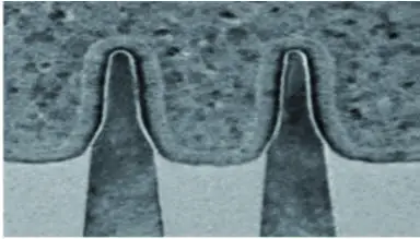
| 14nm vs 7nm FinFET Fin Cross Section TEM | |
|---|---|
| GF 14nm | GF 7nm |
 |
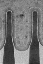 |
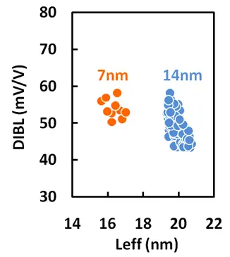
The Fin is pitch is 30nm, meaning quad patterning is being employed here. We also measured a fin height of ~42nm which coincidentally happened to be the same height as Intel’s 14nm and their newly introduced 22FFL. The fin shape has been carefully optimized to improve the short-channel effects. The graph below clearly shows the improvement in DIBL vs the Leff when comparing the 7nm node to their 14nm process due to the fin profile optimizations that were done. For the same DIBL levels, there is a gain of roughly 4nm for the Leff.
This is also their 2nd generation of their (actually IBM’s) multi-workfunction (multi-WF) approach for device Vt. The multi-WF (in their 14nm they introduced dual-WF) process is used to generate widely-spaced Vts for both N/P without relying on doping to create the Vt separation. The underlying concept is undoped fins. Undoped fins introduce the benefits of higher mobility gains as well as it reduces the random dopant fluctuation (RDF)-induced threshold voltage (VT) variability (RDF-Vt mismatches). They first introduced this process with their 14nm SOI which had 4 undoped fins and 4 workfunction materials. In their 7nm this was enhanced to cover the entire range of Vts and this was enabled through the integration of eight additional workfunction materials.
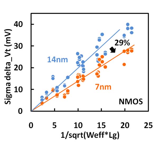
GlobalFoundries 7nm covers the entire Vt range from very low leakage devices to very high performance. In the graph above GlobalFoundries compared their 14nm undoped fins against their 7nm undoped fins. GF reported around 30% lower mismatch which was obtained with this process.
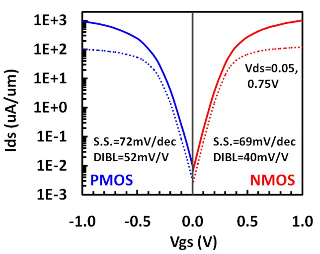
Shown is the reported subthreshold swing of ~70mV/dec and DIBL of ~40/50mV/V for N/P.
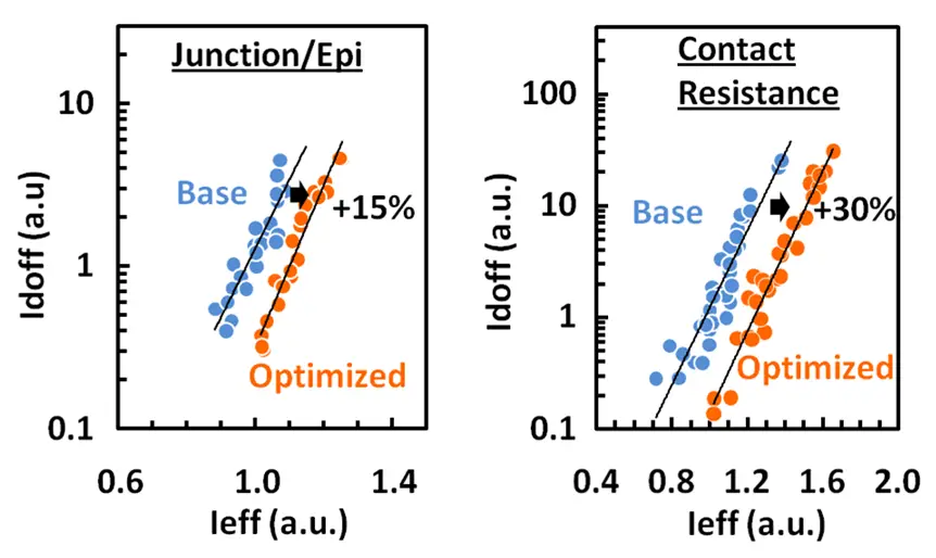
Additionally, GF introduced junction/epi and contact resistance optimizations in order to reduce the FinFET parasitic resistance. Those optimizations were required for them to reach the targeted effective current levels. The left graph shows the Idoff vs the Ieff which shows that vs the baseline, there is 15% improvement in the external resistance from the junction depth optimization doping. To improve the other components that affect the external resistance, GF optimized the interface between the contact and the epi. The graph on the right shows the Idoff vs the Ieff for the base case vs the contact resistance reduction optimizations. GlobalFoundries reported 30% improvement over the base case.
–
Spotted an error? Help us fix it! Simply select the problematic text and press Ctrl+Enter to notify us.
–