
IEDM 2017: GlobalFoundries 7nm process; Cobalt, EUV
Efficient Routing
In order to accomplish efficient scaling at the SoC level, it’s not enough to just scale the cell. GlobalFoundries had to rework and optimize their routing rules. Dr. Jagannathan listed a number of optimizations they have done in order to achieve the desired post-route scaling. Those include logic cell design by removing the various blockages, intelligent pin placement, and various routing optimizations. GF did not detail those optimizations any further for us to be able talk about them. All of those optimizations are part of their new ground rules.
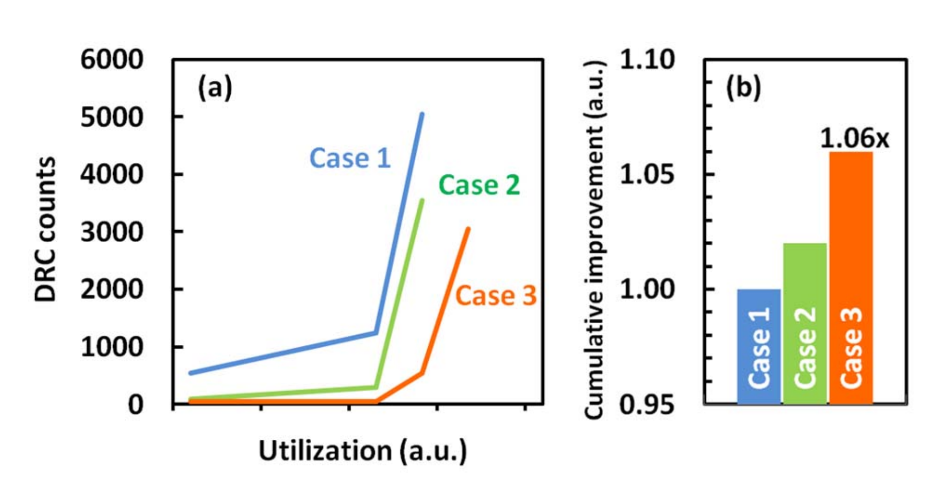
The graph above plots design rule checks (DRC) against utilization of of various design optimization cases introduced where case 2 refers to the cell design optimization and case 3 for the pin optimization. Together, all three optimizations were necessary in order for their 7nm process to achieve the 2.8x routed logic density goal.
High-Performance Cells
The 2-fin cell isn’t suitable for all applications and for high-performance computing GlobalFoundries 7nm process also offers a 4-fin logic cell.

This cell is a 9-track cell meaning the cell height is 360 nm. More fins alone is not enough and for those high-performance applications there is a need for larger power grids and large wires. For that, whereas the 2-fin 6T logic cells featured minimum Mx pitches for height scaling, the 4-fin 9T logic cell makes use of larger wire dimensions and increased contact sizes and vias. This was done in order to limit the IR drop and maximize performance. GlobalFoundries developed simultaneous support for a large range of wide wires and large contact and vias that make use of SADP for power grid, high-performance, and also custom high-speed analog and mix signal work.
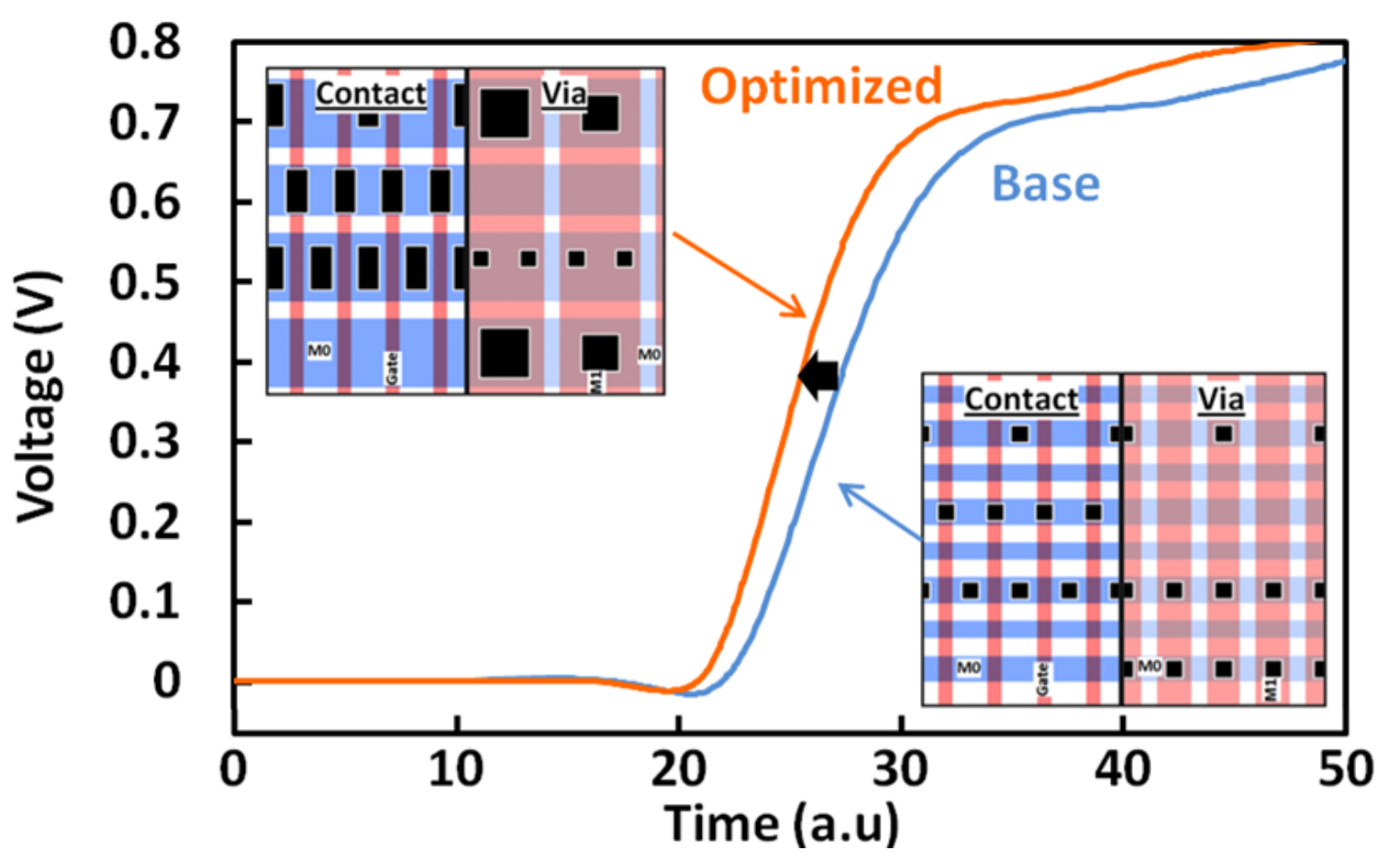
Wide wires and large contacts greatly benefits applications such as high-speed buffer designs or low RC intra-blocking wiring in large memories. The graph above illustrates the impact of a buffer designed for high-speed SerDes (HSS) application. The SPICE voltage trace shows a 30% improvement in the rise time when optimizing the design using wide wires and contacts.
The extra drive strength that is available through the extra fins allows them to scale to higher frequencies that are a necessity for high-performance applications.
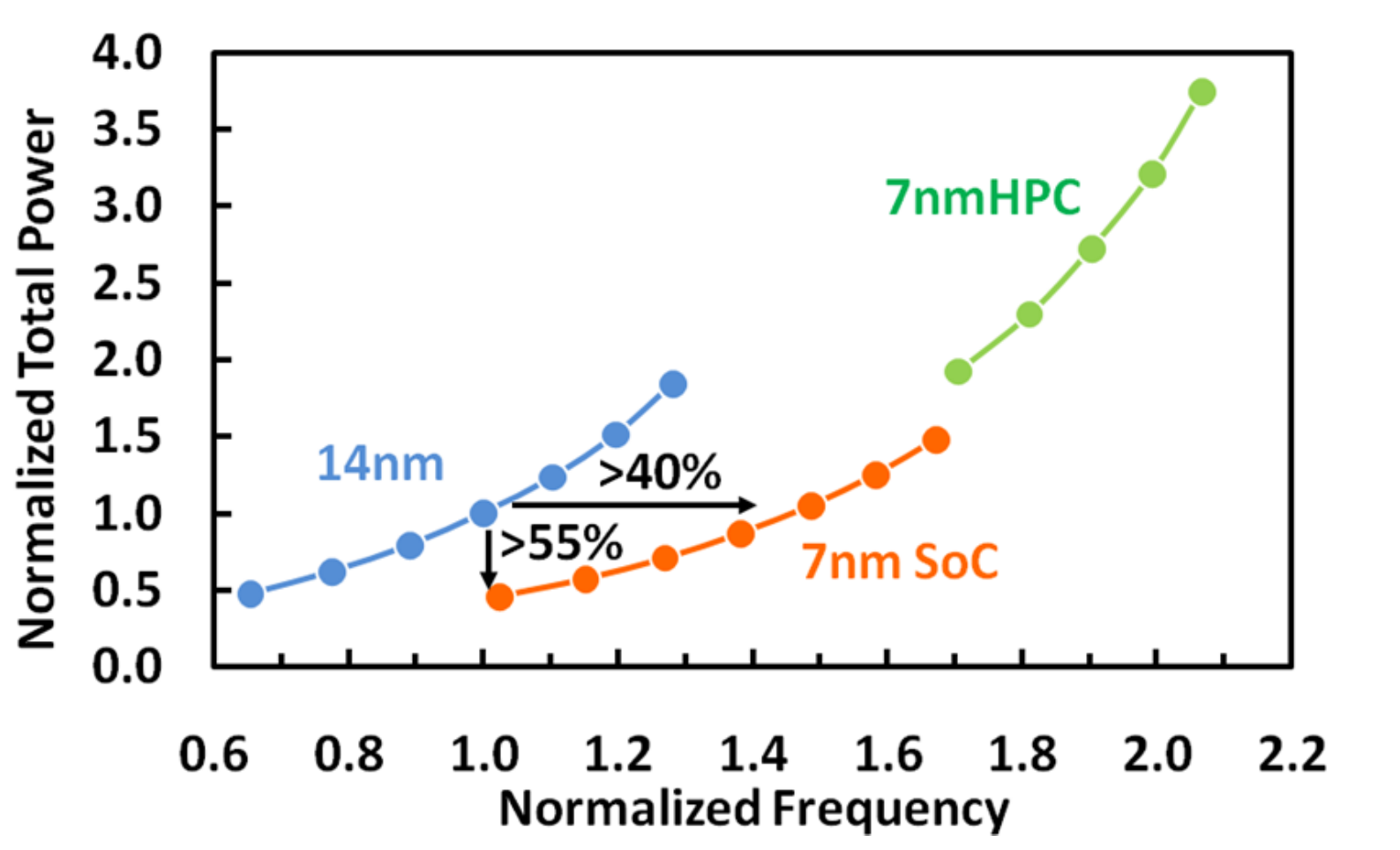
The graph above shows the performance extendibility achieved by the 4-fin logic cell. This is a very important requirement for high-end server applications that focus on single-thread performance (e.g., IBM’s z/Architecture and POWER).
–
Spotted an error? Help us fix it! Simply select the problematic text and press Ctrl+Enter to notify us.
–