
IEDM 2017: GlobalFoundries 7nm process; Cobalt, EUV
SRAM
As is usually the case when reporting on a new process, GlobalFoundries presented their SRAM bitcell offerings. Two cells were presented, a high-performance cell (PU:PG:PD = 1:2:2) and a high-density cell (PU:PG:PD = 1:1:1).
| GF 7nm SRAM | |||
|---|---|---|---|
| Cell | Area (14nm) | Area (7nm) | |
| HP | 0.080 µm² | 0.0353 µm² | |
| HD | 0.064 µm² | 0.0269 µm² | |
Note that the SRAM sizes for their 14nm came from their 2017 IEEE Symposium on VLSI Technology presentation. The 7nm SRAM was reported at this IEDM.
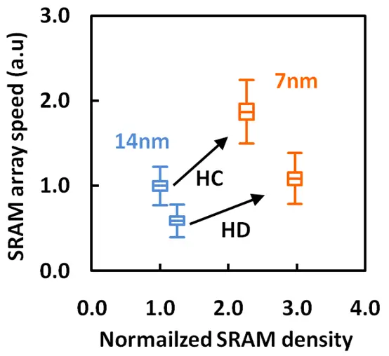
In the graph above GlobalFoundries compares the 14nm reference node to their 7nm in normalized density and array speed. What’s immediately obvious is just how well the two cell (1-1-1 and 1-2-2) scaled from the 14nm to the 7nm process. GF reported over 2.3x improvement in array density. Similarly, they also reported 2x in array speed performance. Jagannathan explained that the array speed improvement came from lower bit line capacitance and significant improvement in the read current. Note that the majority of the read current improvement came from the reduction in RDF-Vt mismatches which we talked about earlier.
Back-End
Two separate metallization stacks were designed for the 7nm process: a general-purpose stack and a high-performance stack. This allows flexibility in applications for anywhere from density to performance.
General-Purpose Stack
The general-purpose stack is 13 levels:
| GF 7nm General-Purpose Stack | |||
|---|---|---|---|
| Layer | Pitch (nm) |
Note | TEM |
| M0 | 40 | 1x, SADP, Unidirectional | TEM showing the two 2x pitch layers, the three 1x pitch layers, and the FEOL at the bottom. 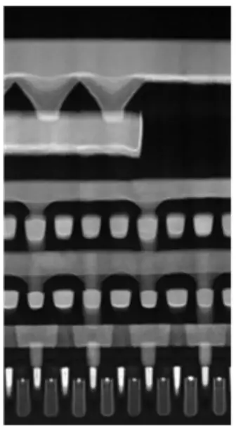
|
| M1 | 56 | 1x, SADP, Unidirectional | |
| M2 | 40 | 1x, SADP, Unidirectional | |
| M3 | 40 | 1x, SADP, Unidirectional | |
| M4 | 80 | 2x, Single, preferred orientation | |
| M5 | 80 | 2x, Single, preferred orientation | |
| M6 | 80 | 2x, Single, preferred orientation | |
| M7 | 80 | 2x, Single, preferred orientation | |
| M8 | 80 | 2x, Single, preferred orientation | |
| M9 | 80 | 2x, Single, preferred orientation | |
| M10 | 128 | 3.2x, Single Bidirectional | |
| M11 | 128 | 3.2x, Single Bidirectional | |
| M12 | 720 | 18x, Single Bidirectional | |
| M13 | 720 | 18x, Single Bidirectional | |
As a side note, their paper says the general-purpose stack has 13 interconnect layers but it really has 14 layers when we count M0. There is an advanced MIM cap available for the M13 layer used to decouple strong power supply.
High-Performance Stack
For the high-performance stack GlobalFoundries developed an 18-layer metallization stack. For this stack there was a need for very low resistance in the power grid and for that GF added optional layers available at 6.4x, 9x, and 60x. Note that the advanced MIMcap is available here at the 60x level.
| GF 7nm Heigh-Performance Stack | ||
|---|---|---|
| Layer | Pitch (nm) |
Note |
| M0 | 40 | 1x, SADP, Unidirectional |
| M1 | 56 | 1x, SADP, Unidirectional |
| M2 | 40 | 1x, SADP, Unidirectional |
| M3 | 40 | 1x, SADP, Unidirectional |
| M4 | 80 | 2x, Single, preferred orientation |
| M5 | 80 | 2x, Single, preferred orientation |
| M6 | 80 | 2x, Single, preferred orientation |
| M7 | 80 | 2x, Single, preferred orientation |
| M8 | 80 | 2x, Single, preferred orientation |
| M9 | 80 | 2x, Single, preferred orientation |
| M10 | 128 | 3.2x, Single Bidirectional |
| M11 | 128 | 3.2x, Single Bidirectional |
| M12 | 256 | 6.4x, Single Bidirectional |
| M13 | 256 | 6.4x, Single Bidirectional |
| M14 | 360 | 9x, Single Bidirectional |
| M15 | 360 | 9x, Single Bidirectional |
| M16 | 2,400 | 60x, Single Bidirectional |
| M17 | 2,400 | 60x, Single Bidirectional |
40nm restriction, Cobalt
Transistor geometry is always the center of attention, however it’s the interconnects that we should really be talking about. The sad reality is that interconnect scaling is facing major roadblocks and are lagging way behind the transistor. One thing you might notice is how the pitches were restricted to 40nm in order to allow for dual-patterning instead of quad-patterning. The reason for this is the extra flexibility that double patterning allows over quad patterning. In particular, SADP is better suited for allowing customers to choose very wide wires for one applications and vary narrow wires for another. As you scale the device, you also scale the contacts. GlobalFoundries introduced cobalt for the trench metal contacts. This actually plays out in two different ways. For small layouts, the vertical resistance dominates. In those cases GF reported an improvement of over 40%. When those contacts are used for the local interconnects, the horizontal resistance becomes important. In those cases, GF reported an improvement of around 80% when switching to cobalt. All this flexibility is lost had they shrunk the pitches further. Unfortunately, this decision left them with less than ideal interconnect in many situations. Those types of sacrifices are required for a foundry that needs to provide customers with flexibility whereas a company such as Intel can achieve superior routing by allowing itself to be more aggressive at the cost of higher restrictions and higher complexity.
For both stacks GF achieved capacitance reduction from low-K fill optimization as well as the etch stop layer. Compared to their base process, GF reported around 10% capacitance improvement from the ILD stack optimization. They did introduce cobalt, but only for the liner and the caps on the SADP layers. They claimed this improved the electromigration by 100x over their 14nm reference node. Jagannathan noted that “without those optimizations, the power grids at 7-nanometer ground rules would be 3x larger. But with this improvement in place, the power grid can actually be 4x smaller in 7nm compared to prior node.”
–
Spotted an error? Help us fix it! Simply select the problematic text and press Ctrl+Enter to notify us.
–