
TSMC Q4: 7nm Dominates Revenue, Preps 5nm Ramp, 6nm By EOY
Yesterday, TSMC reported its fourth-quarter earnings. Despite a slow first half, the foundry experienced a rebound in the second half of the year, finishing the fourth quarter on a strong note with net revenue of $10.39 billion, beating guidance by over $100 million. TSMC attributed the increase of 8.3% to high-end smartphones, initial 5G deployment, and HPC-related applications using the company’s latest leading-edge 7-nanometer process.
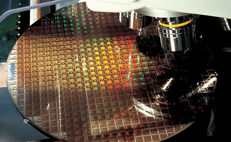
TSMC 7-nanometer process entered production in 2018 and has continued to ramp up throughout 2019 with higher capacity. In Q4, it now accounts for 35% of total wafer revenue shipped. This is the second-highest wafer share by revenue of any node in the past decade – only beaten by the 28-nanometer node during a single quarter. 2019 started off on a weak start with lower-than-expected utilization of its 7-nanometer node. In the chart below this correlates to a small dip in the revenue share in the chart below. Year-round, TSMC saw a gross margin decrease of 2.3% primarily due to lower capacity utilization in the first half of 2019. Nonetheless, with N7 entering its 3rd year, it looks like it’s by far TSMC’s most successful node. Its 10-nanometer node, which served as both a half-node and a yield-learning node, is almost entirely gone – representing just 1% of total wafer revenue. TSMC’s first FinFET node, 16 nm, remains a strong and long-lasting node due to its maturity, cost, and ecosystem. This node still accounts for 20% of wafer revenue in the fourth quarter.
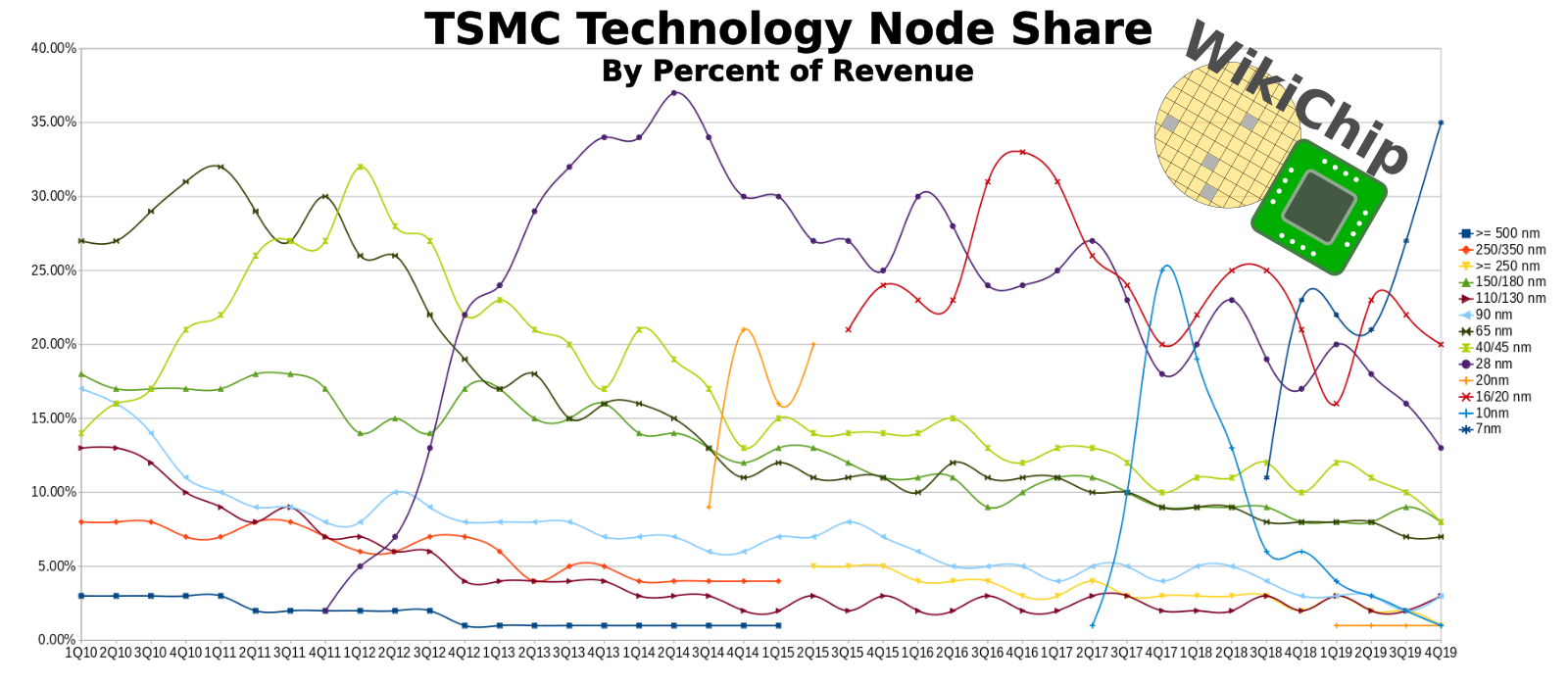
Advanced technologies, which TSMC defines as 16-nanometer and below, accounts for 56% of wafer revenue in Q4, up from 51% in Q3. By the way, on a full-year basis, advanced technologies in 2019 accounted for 50% of all wafer revenue, an increase of 9% (41%) in 2018. The revenue growth in Q4 was driven largely by the smartphone market which saw a 16% increase and HPC with a 6% increase.
It’s worth pointing out that on a full-year basis, smartphones saw a 12% growth while HPC actually saw a significant decline of slightly over 8%. If you were to break down what’s going on in the HPC segment, it is cryptocurrency-related ASICs that drove the overall decline. TSMC says if you were to exclude cryptocurrency products, HPC would have actually increased by mid-single-digits in 2019. HPC accounted for 30% of TSMC wafer revenue in 2019 while smartphones accounted for another 49%. AMD has been ramping its entire portfolio of Zen 2-based products on TSMC’s 7-nanometer node over the last year. In the HPC segment, AMD growth is helping pick up the wafer decline from crypto.
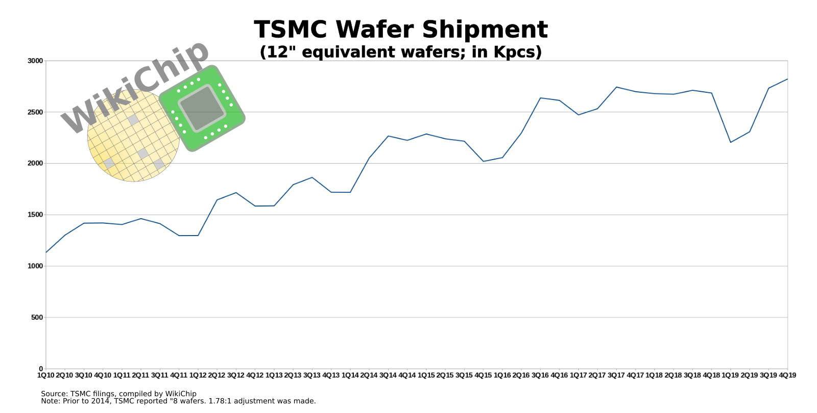
In terms of wafers shipped, TSMC reported a fourth-quarter wafer shipment of over 2.8 million wafers. This is TSMC’s highest wafer shipment ever – beating the previous highest volume of 2.75 million from the third quarter of 2017.
CapEx & Future Nodes
TSMC operating expenses, which include research and development expenses, increased by roughly $120 million due to higher development costs associated with their future 5-nanometer and 3-nanometer nodes as well as due to preparations for their 5-nanometer node ramp. Fourth-quarter capital expenditure reached $5.6 billion. For the full year, TSMC CapEx was $14.9 billion. By comparison, Intel’s capital spending in 2018 was $15.2 billion with around $16 billion planned for 2019 (actual numbers will be announced on January 23). TSMC expects 5G applications and strong HPC demand to drive a strong demand for their advanced technologies in the next several years. For 2020, TSMC expects CapEx between 15 and 16 billion dollars – 80% of which will be allocated to advanced technologies (7 nm, 5 nm, and 3 nm), 10% is allocated for specialty technologies, while the other 10% is allocated for advanced packaging.
N6
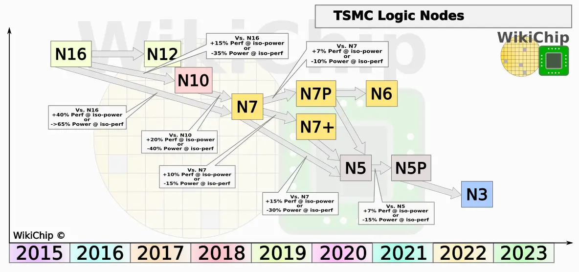
Last year, TSMC announced the N6 node. This is an EUV-based node, but unlike N7+ which is entering its 2nd year of production, N6 is designed to be the easy migration path from N7 as its design rules are fully compatible with N7. In fact, TSMC considers N6 to be part of the “N7 family”. N6 is said to provide around 15-20% higher density with improved power consumption compared to N7, albeit no iso-power or speed comparisons where provided. We believe the density gains are obtained from switching from double diffusion breaks to a single isolation line. TSMC did note that N6 has 1 more EUV layer compared to N7+. TSMC reported that N6 is on track for risk production in the first quarter of this year with volume production expected before the end of the year. The 7 nm family is expected to continue to contribute more than 30% of wafer revenue in 2020.
N5
The N5 node is the next full node after N7 for TSMC. It features an 80% density improvement and a 20% speed gain. This process uses EUV extensively and is on track for volume production in the first half of this year. It’s worth noting that at the earnings call, Dr. C.C. Wei. TSMC CEO said “first half of this year” for the N5 ramp while saying “first quarter of this year” for the N6 risk production. This implies N5 ramp might be in Q2 rather than Q1. “We expect a very fast and smooth ramp-up in the second half of the year driven by both mobile and HPC applications, ” Wei said. “We are confident that 5-nanometer will be another large and long-lasting node for TSMC,” he added. TSMC expects N5 to contribute about 10% of total wafer revenue in 2020. Compared to the initial N7 ramp, at a similar point in the development cycle to where N5 is today, TSMC is reporting slightly fewer tape-outs on its N5, however, they expect the high-volume tape-outs to be comparable.
N3
Like N5, the N3 node is the next full node after N5 for TSMC. Wei stated that N3 will offer another full-node scaling benefit in terms of performance, power, and area compared to N5. “We are working with customers on N3 designs and the technology progress is going well. We have many technology options in development and we carefully evaluate all the different approaches. Our decisions are based on technology maturity, performance, and cost,” Wei said. “We expect our N3 technology to be the most advanced foundry technology in both PPA and transistor technology when introduced.” Given 2021 has the N5P process planned, we expect TSMC N3 to ramp around the 2022-23 timeframe.
–
Spotted an error? Help us fix it! Simply select the problematic text and press Ctrl+Enter to notify us.
–