
Ranovus Odin: Co-Packaging Next-Gen DC Switches and Accelerators With Silicon Photonics
As silicon photonics make their way closer to compute, the first wave of high-bandwidth devices has been centered around long-distance data-center-to-data-center connectivity. Over the last few years, technology grew in popularity within the data center. Bringing optics close to the compute here meant bringing optics to network switches. But switches only gets us so far. More recently, we’ve seen some of the first steps in the industry to bring silicon photonics directly to the processing chips themselves. One such company that’s been working on this technology is Ranovus, an Ontario, Canada based company. Founded in 2012, they have been working on various silicon photonics technologies. Today, they are ready to talk about their impressive technology.
Some of the popular silicon photonics transceiver technologies on the market today, such as the PSM4 QSFP 100G optical transceivers, rely on propagating light over four separate channels. In other words, optical signals travel over four parallel 25Gbps per fibers. With a technique called wavelength-division multiplexing (WDM), multiple wavelengths of laser light can be carried on a single optical fiber. Moving from PSM4 to CWDM4 transmitters meant that there’s now a single fiber pair that can carry 100Gbps vs 4 fiber pairs of PSM4. The way we currently add more wavelengths is by adding more parallel lasers. To provide 16 or even 32 lasers means placing 32 lasers side by side. Assembling the many lasers together incurs a cost, power consumption, and area overhead.
Ranovus has been working on several key technologies that enable their optical products. One of those technologies is a quantum dot-based (comb) laser. A QDL is a special kind of laser capable of generating multiple wavelengths simultaneously from a single chip. Quantum dots are not a new technology, but existing implementations relied on relatively low data rates – on the order of a couple of gigabits per second. Achieving high bandwidth would require a great number of parallel channels. Ranovus says they are able to design a laser with not only a large number of wavelengths but are also able to achieve very high data rates. We are talking 100 Gbps per fiber which is multiple times higher than some of the other technology demonstrations we have seen recently. The key thing to note about their technology is that this is not a lab demonstration. Ranovus’s first laser based on this technology was a 37-wavelength laser. The company demoed the technology back in 2012 and a custom product has since been designed for data center to data center connectivity. This is a fully qualified and in-production product.
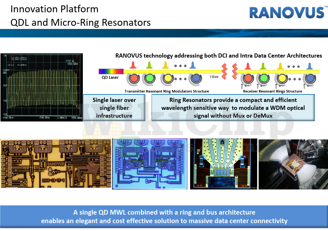
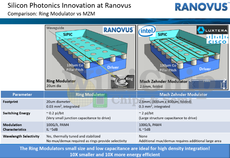
A separate key technology as part of Ranovus’s portfolio is the use of ring resonators. We’ve talked about ring resonators before. Those are effectively wavelength filters that allow them to operate on a single wavelength from the waveguide. Many of the existing technologies on the market today use MZMs such as those productized by Intel and Luxtera (although rings are used by their partner Ayar Labs). The benefits of rings are well-known today including multiple order of magnitude smaller footprint, much higher bandwidth, and much higher energy efficiency.
Ranovus is very product-focus at this point. Their initial financing is slightly different to most other startups – it’s roughly half financed through venture capital and half financed through the Canadian government and NREs from customers. The company received major funding from the Canadian government in 2018 in order to build a co-packaged optics ecosystem around its technology in Canada. They are a relatively small company with about 60 employees cross a number of R&D centers in the US, Canada, and Germany. They have developed their own lasers (quantum dot and quantum well) and have their own laser foundry. Drivers, TIAs, and control chips are developed at their Nuremberg Germany center. Laser, SiPho design, and packaging are done in Ottawa. They are currently focused on two major markets – ethernet switching and disaggregated servers.
Odin 8 platform
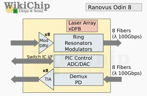
What Ranovus is launching is the Odin 8 Silicon Photonic Engine. The Odin 8 is the base product on top of which more complex products are built. This is the silicon photonics chip with all the divers, modulators, and other connectivity on a single monolithic integrated circuit with the lasers attached to the silicon. There are eight optical channels coming in and eight optical channels coming out.
Each of the eight optical channels is currently capable of 100G/64G/50G PAM4 or 50G/32G/25G NRZ or PCIe Gen 5 or Gen 6. The chip is designed as an electrical-optical converter. On the one side of the chip is a protocol-agnostic interface which can be mapped onto the optical wavelengths on the other side. For example, Odin 8 can map PCIe Gen 5/6 onto optical wavelengths.
Ranovus told us that they have already demonstrated their 800G capabilities as well as validated the protocol-agnostic and low latency optical engine with four major players in the machine learning market.
800G Ethernet
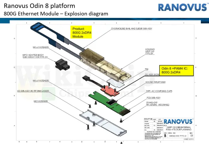
The Odin 8 chip is a fairly generic chip that allows it to go into many different applications. In fact, Ranovus itself is using the Odin 8 to develop 800G Ethernet modules. They have partnered with two companies for the PAM4 IC which will be packaged together with the Odin 8 to form a complete optical engine for 800G Ethernet module. The Odin 8 is validated. The company plans on sampling its 800G Optical Engine and module once the 100G PAM4 ICs are made available. They expect market deployment to start in the first quarter of next year.
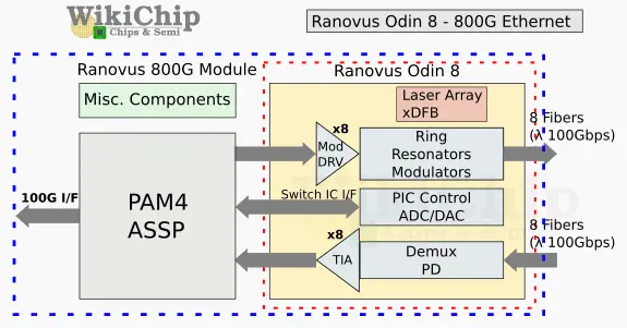
The full 800G Ethernet Optical Engine comprises the Odin 8 (highlighted in red) and the PAM4 IC. It’s worth highlighting just how simple the module itself is with almost no other component on it which should make it a very cost-effective product.
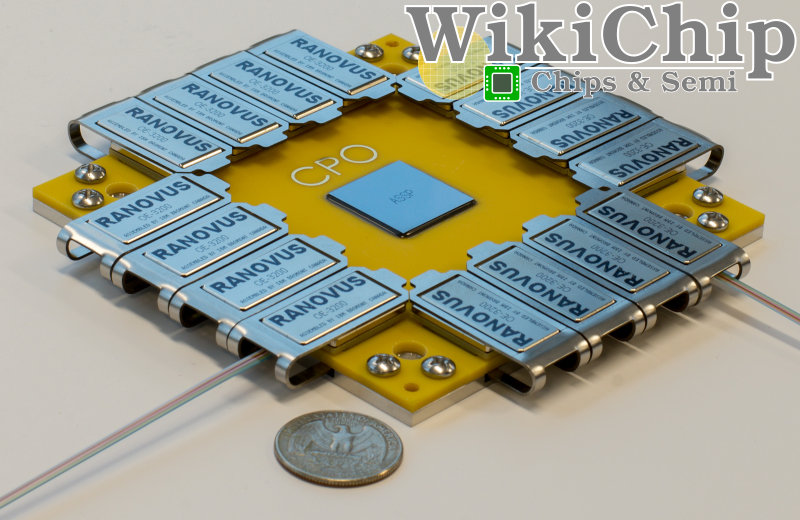
Odin 32 – 51.2 Tbps
One of the nice things about the Odin 8 chip is that it’s compact enough to allow scaling. As part of this announcement, Ranovus is also announcing the Odin 32 which co-packages the Odin 8 to scale to a large number of optical fiber channels. In the co-packaging below, you can see how multiple Odin 8 chips can be clipped onto a single co-packaged product. Ranovus has collaborated with a number of industry partners to make the whole technology work. They have partnered with IBM for their fiber V-groove interconnect packaging technology which is an assembly technique used to interface optical fibers to photonics devices. “This process makes use of passive alignment techniques and achieves low insertion loss across a wide spectral range in both the O-band and C-band regimes.” They are also collaborating with TE for their co-packaged (CP) fine pitch socket interposer technology and Senko for their fiber optic connectivity technology.
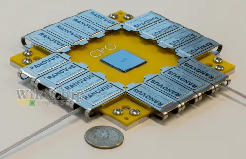
Electrical signals from the center chip go into the Odin 8 chips which get converted into optical to be sent out. The only difference between this large co-packaged chip and the individual Odin 8 modules is the laser which brings light is on the outside serving as a remote laser source. In the single Odin 8 chip we described earlier, the laser is directly attached to the silicon photonics IC. The laser taken out means more lasers can be fed in. In this product, the Optical Engines provide up 3.2 Tbps of bandwidth (8x400G FR4) which is four times the capabilities of the Odin 8. A fully populated module is currently capable of offering is an impressive 51.2 Tbps of peak bandwidth.
Because the individual Odin 8 chip uses a protocol-agnostic interface, the chip in the middle of that package can be any chip with any electrical interface protocol. Although the first few products to take advantage of the full 51.2 Tbps will most likely be Ethernet network switches. You can drop an FPGA in the middle and offer custom connectivity products. This is exactly what Ranovus is trying to do. Ranovus says that a number of customers are testing and validating this product for Ethernet switches solutions as well as accelerators such as FPGAs, NPUs, and GPUs that need high-capacity scale-out capabilities. The connections on that package don’t have to be 100G or all-fiber either. For example, an Nvidia GPUs currently use 25G NVLinks, therefore a more appropriate Odin 32 configuration could be a number of local copper connections and a number of 25G optical fan-outs.
The packaging options for the Odin 32 can also vary by product. There are smaller configurations for products that only need a few connections instead of the full 16 chips such as the flagship package shown above. In fact, this can be scaled down to just a single Odin 8 chip operating at 800 Gbps to 3.2 Tbps which is sufficient for many of today’s GPUs and NPUs.
A number of products based on the Odin platform are expected to be announced by late next year.
–
Spotted an error? Help us fix it! Simply select the problematic text and press Ctrl+Enter to notify us.
–