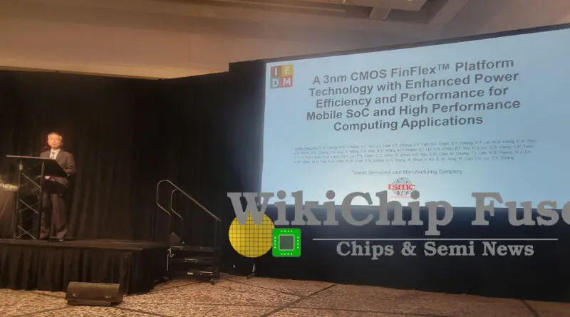
TSMC N3, And Challenges Ahead
A Look At TSMC N3 Process
Read more
Your Chips and Semi News
A Look At TSMC N3 Process
Read more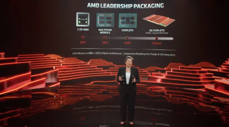
[Subscription] A technical look at AMD’s 3D-Stacked V-Cache
Read more
SiFive introduces a new high-performance coprocessor interface targeting custom accelerators; scores design wins from Google, NASA.
Read more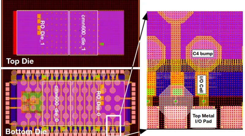
With hybrid bonding inching towards production, here’s a look at Trishul, Arm’s first exploratory test chip – in collaboration with GlobalFoundries – that demonstrates the feasibility of high-density 3D stacking using Arm’s CoreLink CMN-600 extended to 3D.
Read more
AMD recently unveiled 3D V-Cache, their first 3D-stacked technology-based product. Leapfrogging contemporary 3D bonding technologies, AMD jumped directly into advanced packaging with direct bonding and an order of magnitude higher wire density.
Read more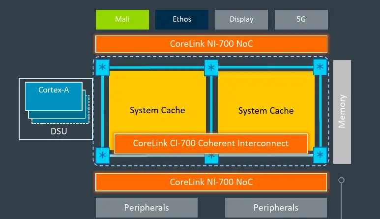
Arm is introducing a new cache-coherent and SoC-level interconnects, the CoreLink CI-700 & NI-700.
Read more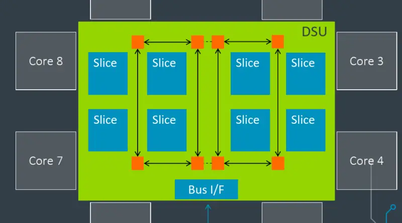
Arm introduces its new DynamIQ Share Unit 110 for new Armv9 CPUs
Read more
Arm’s CMN-700 is the company’s latest high-performance cache-coherent mesh interconnect for the server market, enabling SoC designs with twice as many cores, as much as half a GiB of cache, dozens of memory controllers, and support dozens of cache-coherent accelerators, chiplets, and processors.
Read more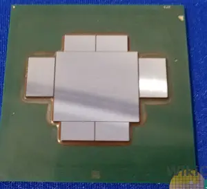
A look at ODI, a new family of packaging interconnect technologies that bridges the gap between Intel’s EMIB (2.5D) and Foveros (3D) by providing the flexibility of an EMIB in 3D with additional benefits of thermal & power.
Read more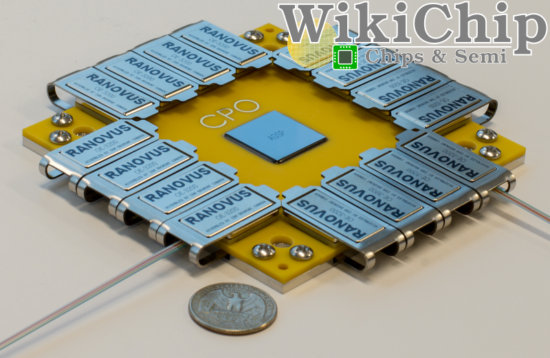
Ranovus launches its Odin platform, a multi-wavelength Quantum Dot Laser (QDL) based silicon photonic engine which includes 800Gbps to 3.2Tbps single-chip engines as well as co-packaged optics scaling up to 51.2Tbps for next-generation data center switches and other HPC compute chips that require high bandwidth capacity.
Read more