7nm Boosted Zen 2 Capabilities but Doubled the Challenges
The transition to 7 nm greatly enhanced AMD silicon capabilities but introduced new drastic design challenges that required new place and route methodologies and wire engineering.
Read moreThe transition to 7 nm greatly enhanced AMD silicon capabilities but introduced new drastic design challenges that required new place and route methodologies and wire engineering.
Read moreA dive into the Rosetta ASIC switch, the engine behind Cray’s new Slingshot interconnect powering the upcoming Shasta exascale supercomputers.
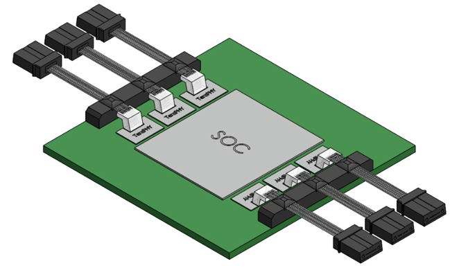
Read moreIntegrated photonics has long been considered a holy grail for communication. Ayar Labs TeraPHY chiplet represents a major step forward through the co-packaging of the optical interface along with an SoC.
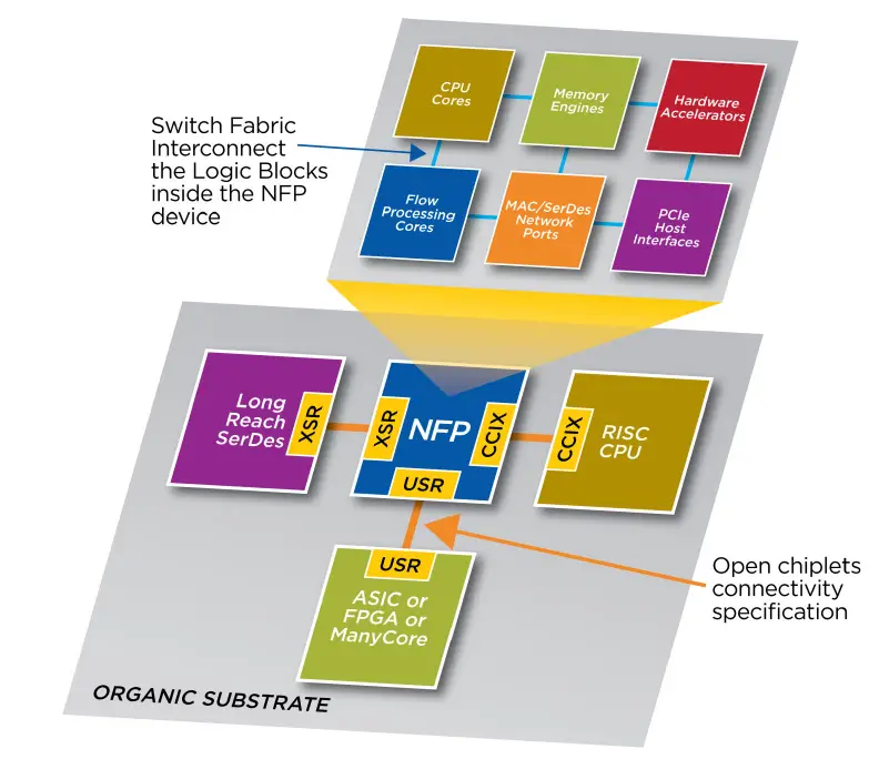
Read moreA look at a Bunch of Wires, a new open standard chiplets interconnect being proposed by the OCP ODSA group intended for standard organic multi-chip packages as a cheaper alternative to silicon interposers and bridges.
Read moreJumping ahead of emerging semiconductor trends, the OCP new Open Domain-Specific Architecture subgroup makes a push for an open and standardized chiplet interface and marketplace.
Read moreTSMC leverages existing silicon in the CoWoS process to improve the power delivery system of high-performance applications through new, deep trench capacitors, codename iCAPs.
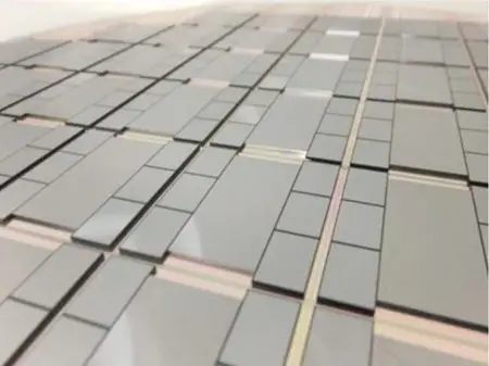
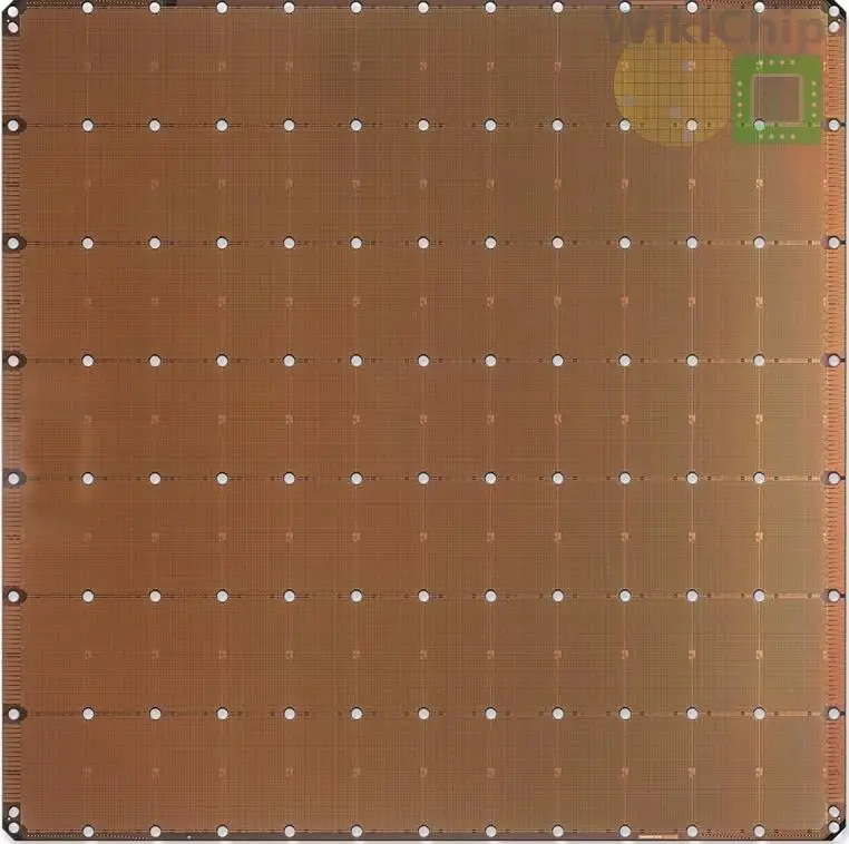
Read moreA look at Cerebras Wafer-Scale Engine (WSE), a chip the size of a wafer, packing over 400K tiny AI cores using 1.2 trillion transistors on a half square foot of silicon.
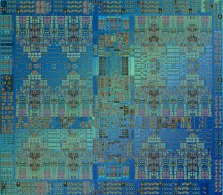
Read moreIBM adds a third variant of POWER9, the POWER9 Advanced I/O (AIO) processor which incorporates the Open Memory Interface (OMI), a new open memory-agnostic interface.
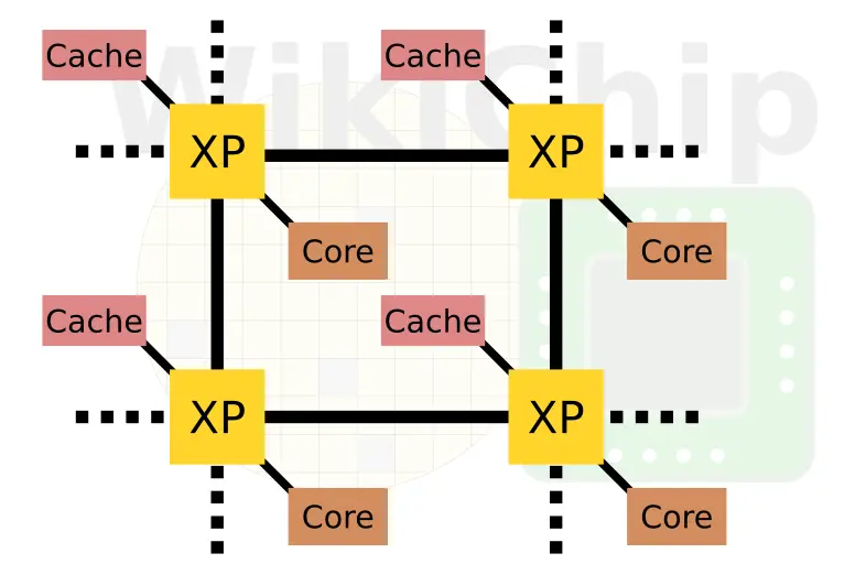
Read moreGlobalFoundries and Arm demonstrate a 3D mesh interconnect design using highly-dense hybrid bonding 3D stacking technology intended for HPC applications.
Read moreAt look the Ice Lake Thunderbolt 3 integration, Intel’s biggest integration since the graphics on Sandy Bridge.
Read more