
IBM Adds POWER9 AIO, Pushes for an Open Memory-Agnostic Interface
Over the summer, Jeff Stuecheli was back at Hot Chips to talk about IBM’s next-generation POWER processor. The company had originally planned POWER10 for next year but has since delayed POWER10 to 2021. Next year, IBM will be rolling out a new third variant of POWER9 with an advanced I/O interface.
From Centaur to the Open Memory Interface
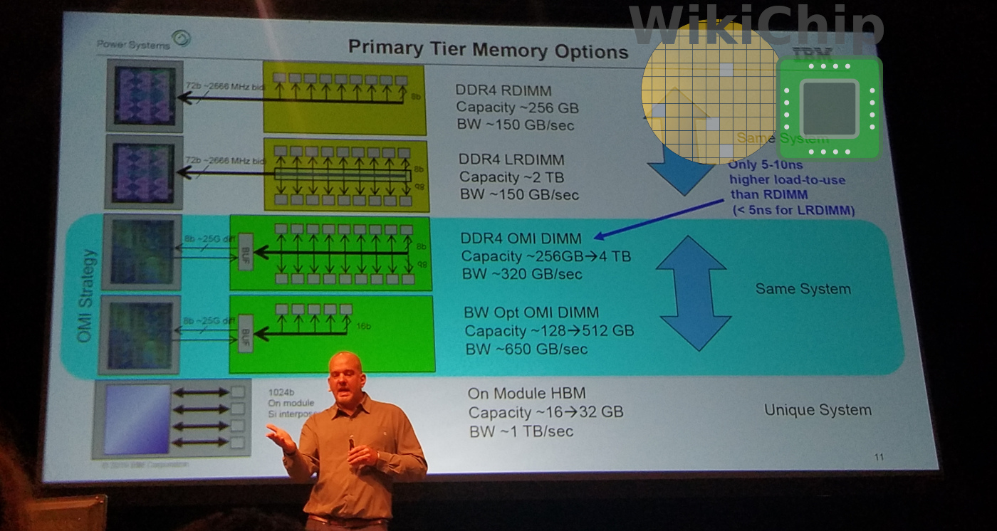
Recent server processors come with up to eight DDR4 memory channels. The industry is already looking at ten channels. While we will see ten memory channels in future products, it’s unlikely adding more channels will help meet future workload requirements. Part of the challenge comes from the parallel interface nature of the technology as well as the growing board requirements. The Open Memory Interface (OMI) is one of the alternatives to traditional parallel direct-attached DRAM. It is a new emerging JEDEC standard serial interface being promoted by IBM.
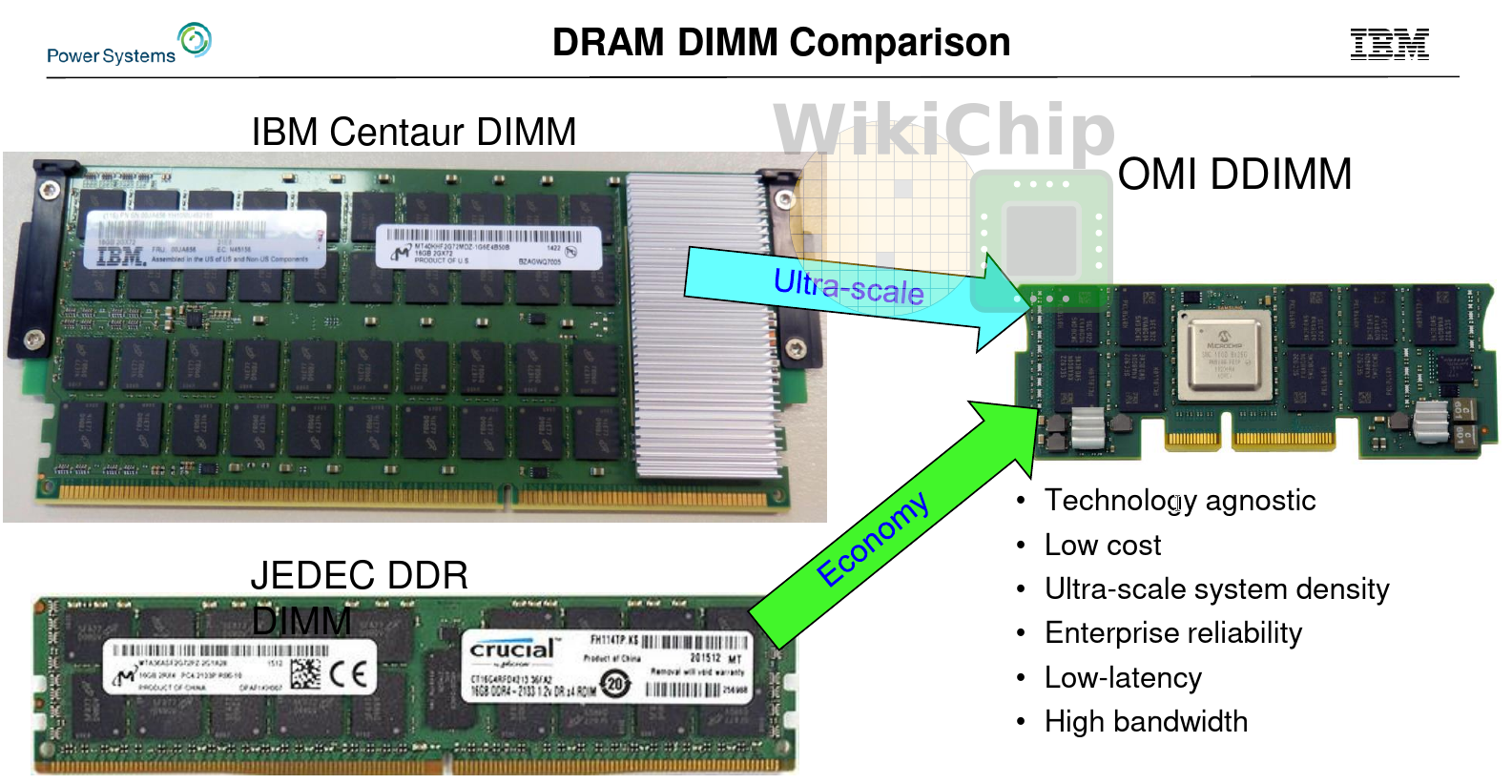
Our readers who follow IBM POWER closely are probably familiar with the POWER9 Scales Up which was announced last year. The POWER9 (and 8) SU system utilizes the Centaur memory buffer chip.
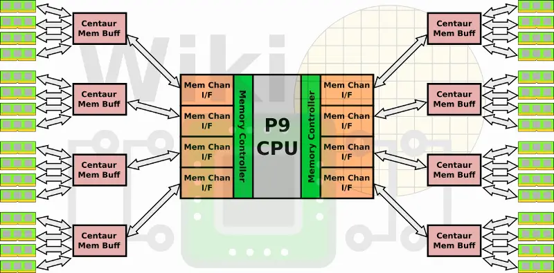
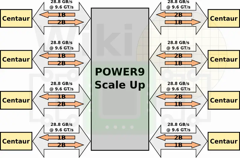
In the POWER9 SU, each memory channel is capable of 1B write + 2B read at 9.6 GT/s or 28.8 GB/s for a total aggregated bandwidth of 230 GB/s across all eight channels. Since every Centaur chip has 16 MiB of L4 cache, there is a total of 128 MiB of L4 cache that can speed critical operations.
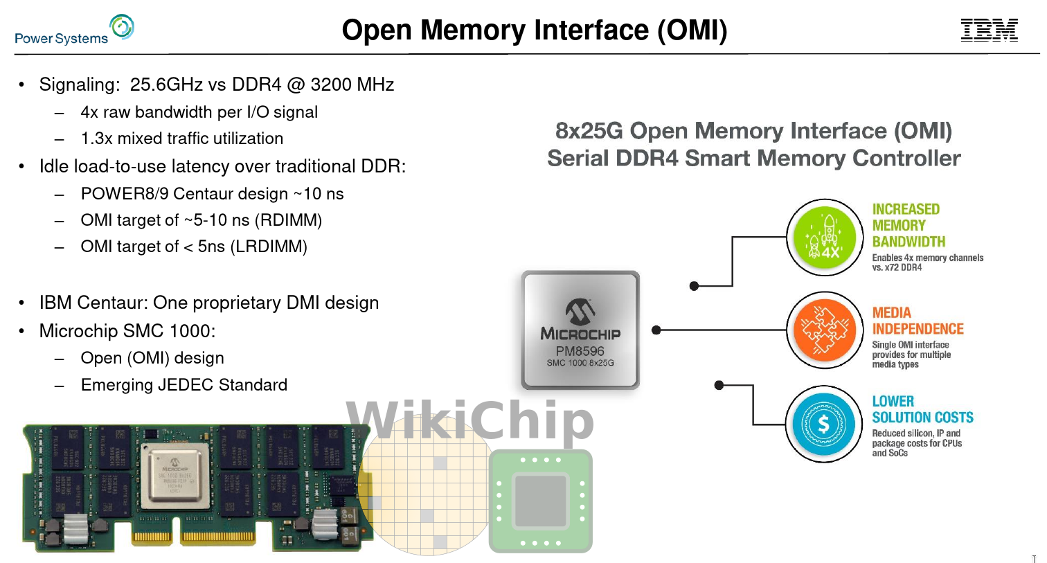
This is where the Open Memory Interface (OMI) comes in. OMI is an open, standardized version of Centaur. Whereas Centaur uses a proprietary protocol, OMI uses an open one – loosely borrowing the memory semantics subset of the OpenCAPI 3.1 standard from the OpenCAPI Consortium. Additionally, there are some other changes. for example, OMI itself is much more light-weight, allowing for smaller devices. The latency requirements have also improved. Essentially, OMI allows IBM to commoditize what was previously a rather expensive technology using Centaur.
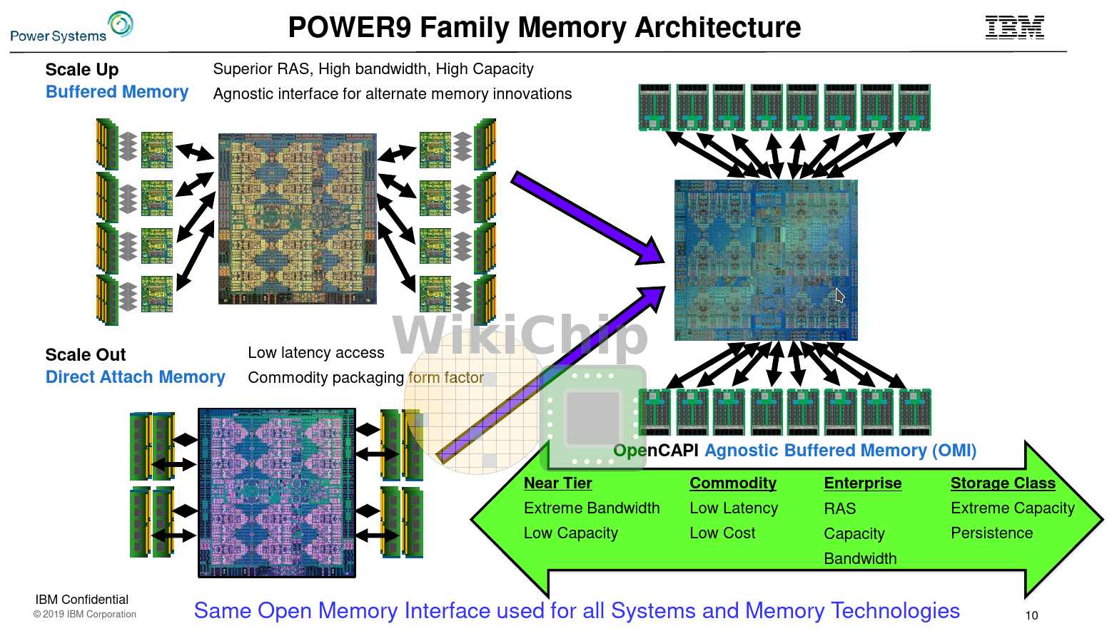
Like Centaur, OMI is memory agnostic. The memory scheduler itself is on the buffer chip; memory requests from the CPU are a simple load and store address requests. Ordering requirements, memory organization, conflicts, and electrical standards are all abstracted. The decoupling of the actual memory allows the DIMM to integrate whatever the system designer wants. It can be used with GDDR, DDR, and various emerging storage-class memories. It could potentially have a private memory hierarchy for better capacity and performance (e.g., having an L4 cache just like the Centaur chip).
On the same system with the same amount of silicon dedicated to memory, the bandwidth/mm² advantages are quite clear. Going from parallel to serial means you can reduce the pin-count from as high as 300 to 75 – allowing for up to four times the bandwidth density. IBM dies are huge (> 700 mm²) which allows them to pack a lot of PHYs. The bandwidth density is much more advantageous for smaller ASICs that don’t have a large amount of silicon that could be dedicated to memory.
Compared to the standard direct-attached DDR4, with an OMI DDR4 DIMM, you are looking at triple to quadruple the bandwidth at the cost of 5-10 ns higher load-to-use than RDIMM. Though the slightly added latency might seem impactful, it’s worth taking a step back and looking at the latency trends of recent systems such as Intel Skylake-SP and AND Rome. For a chip such as AMD Rome, OMI would, in theory, enable them to iterate from DDR4 to DDR5 much more quickly while supporting potentially new non-volatile DIMMs – all without respinning the die. The demand for bandwidth is certainly more important. IBM says that currently, the highest bandwidths OMI is reasonably capable of is around 650 GB/s which is considerably higher than anything else on the market – bar expensive HBM solutions that come in very limited capacities.
Open-Source Reference Design
IBM contributed an open-source reference design of an OMI device under the Apache License, Version 2.0. A reference OMI device with 2 DDR4 memory ports can be found on GitHub. IBM also contributed an example OMI Host design which can be found here.
POWER9 AIO
The first processor to support OMI is the IBM POWER9 Advanced I/O (AIO) processor which will start shipping next year. The POWER9 AIO replaced the four differential memory interface (DMI) channels with eight OMI channels with a data rate of 25 GT/s. This gives the chip a peak theoretical memory bandwidth of 650 GB/s. Additionally, the new chip has upgraded the Nvidia NVLink interface (presumably NVLINK 3.0 although IBM didn’t specifically call that way) as well as support for OpenCAPI 4.0.
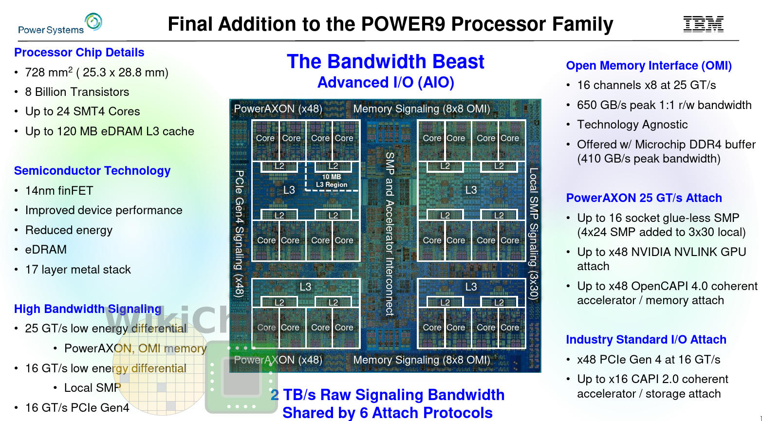
All in all, the POWER9 AIO variant doubles the total aggregated bandwidth of the system over the scale-up variant. This allows them to pack the same amount of bandwidth as direct-attached DDR4 memory in one-sixth of the silicon area.

DDR4 OMI DIMM
The first OMI product on the market was already announced by Microchip. The product announced is the SMC 1000 8x25G, a standard-compliant 8b OMI chip that can interface with 72b DDR4-3200. In collaboration with Micron and Samsung, various 84-pin Differential Dual-Inline Memory Modules (DDIMM) will be offered with capacities ranging from 16 GiB to 256 GiB. The new DDIMMs will conform to the DDR4 and draft JEDEC DDR5 standards.
The new SMC 1000 demonstrates better latencies than IBM Centaur. Whereas Centaur had around 10ns of additional latency, the new Microchip OMI controller offers less than 4ns incremental latency over standard integrated LRDIMM DDR controller. The latency was obtained by eliminating all the asynchronous interfaces as well as through early address pre-decode processing. Additionally, read memory bypasses CRC, using deferred errored. On error, replay occurs by which time the error has already been corrected.
Derived WikiChip Articles: POWER9 Microarchitecture, Centaur.
–
Spotted an error? Help us fix it! Simply select the problematic text and press Ctrl+Enter to notify us.
–