
A Look at Intel’s 10nm Std Cell as TechInsights Reports on the i3-8121U, finds Ruthenium
Early last month, Intel quietly launched a somewhat odd 10 nm part. This processor was shipped in limited quantities in a Lenovo IdeaPads 330. The chip is based on the Cannon Lake microarchitecture but comes with a disabled GPU. Lenovo fixed this by dropping an AMD Radeon RX 540 in there. Lucky for us, TechInsights has managed to get their hands on that laptop and have done an analysis of the chip.
Package, Die Size
As far back as just a few years ago when Broadwell was introduced, Intel was very transparent about their process technology, architecture, and chips. Packaging, die size, and other technical information was abundant.
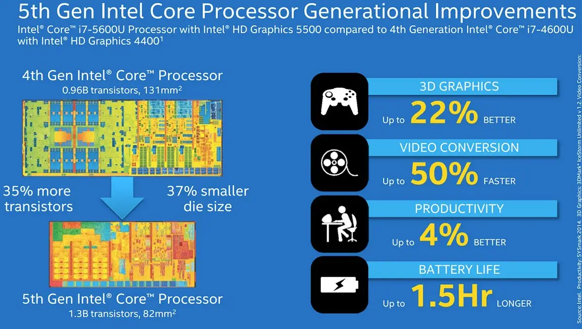
Unfortunately, over the last few years, it’s been missing. Intel has been increasingly light on technical details. Trivial information such as die size and transistor count is now confidential. Fortunately, technology intelligence companies such as TechInsights have been instrumental in demystifying some of the details.
Techinsights has confirmed the chip in the Lenovo IdeaPad 330 is the 10nm Cannon Lake Core i3-8121U, s-spec ‘SRCVC’. They have not mentioned a die size but since Intel revealed that the BGA packaging size is 45mm x 24mm, we can do the math ourselves. We have calculated the die to be 8.2 mm by 8.6 mm for a total area of ~70.52 mm². In fact, Ian Cutress over at AnandTech managed to calculate that exact die size from the photo that was shot at Intel’s Tech Day China last year.
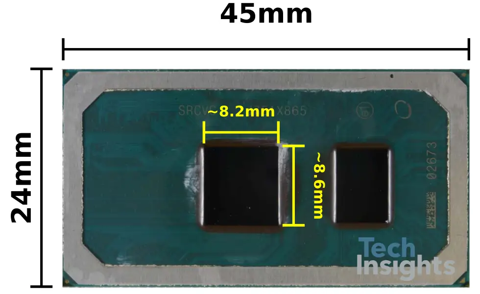
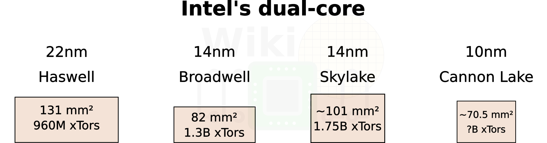
At ~70.52 mm², the Cannon Lake die appears to be the smallest dual-core die Intel has ever made, at least as far as the “big cores” are concerned.
Standard Cells
Earlier this year, WikiChip was able to confirm with Intel the exact layout of their 10nm cells during ISSCC 2018. Given the ongoing confusion of the track design, we have decided to take this opportunity to fully explain the cell design.
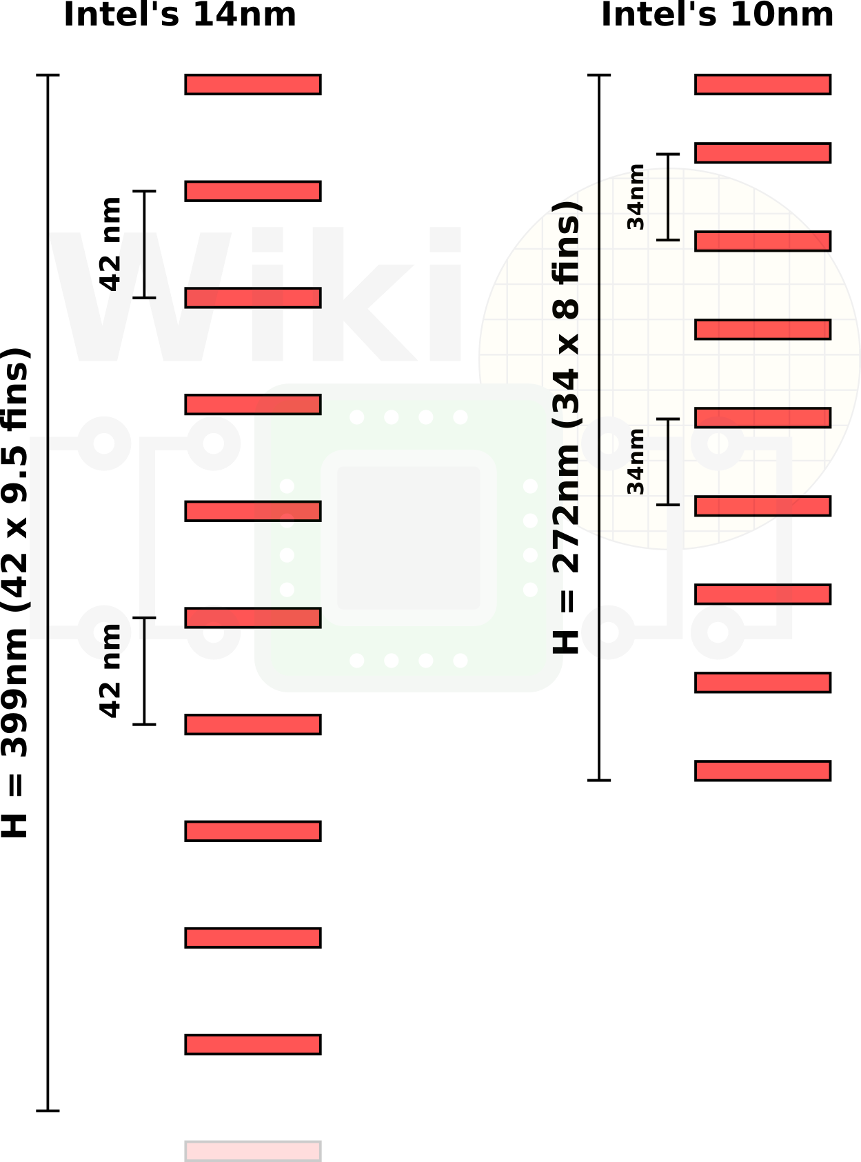
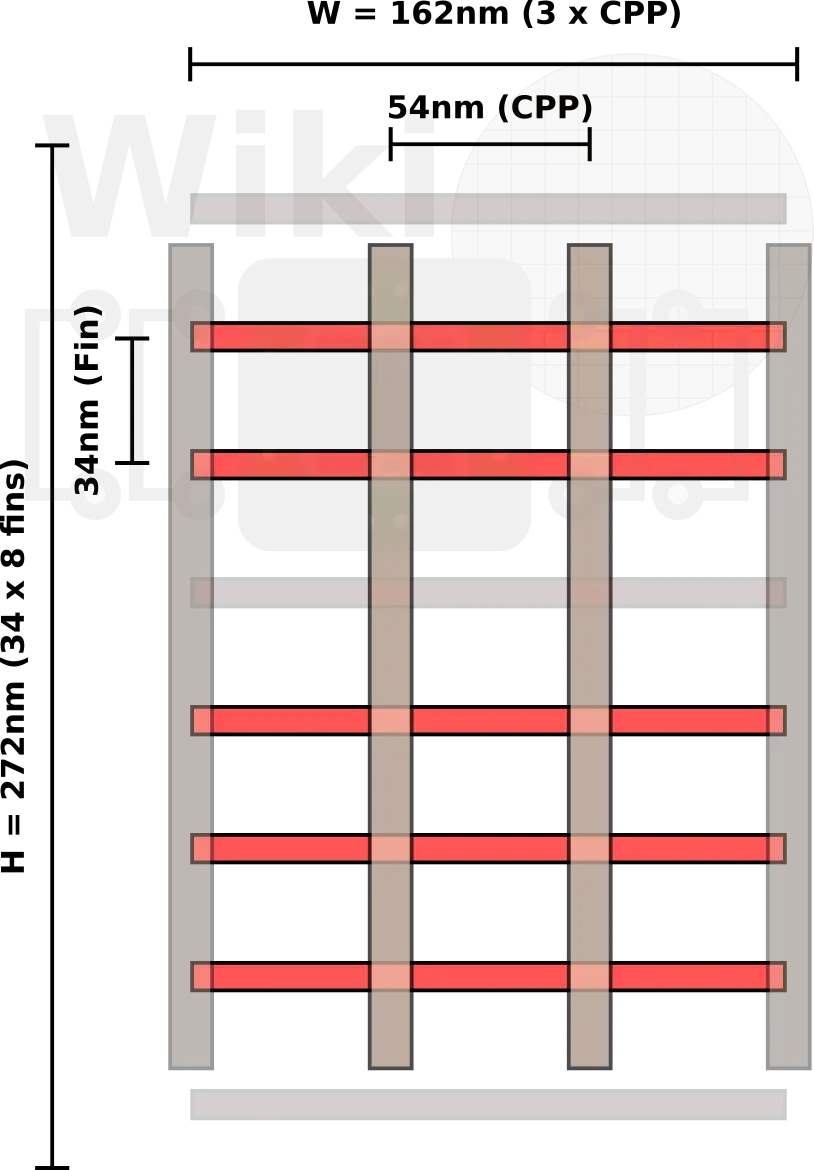
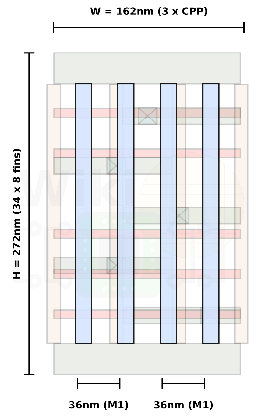
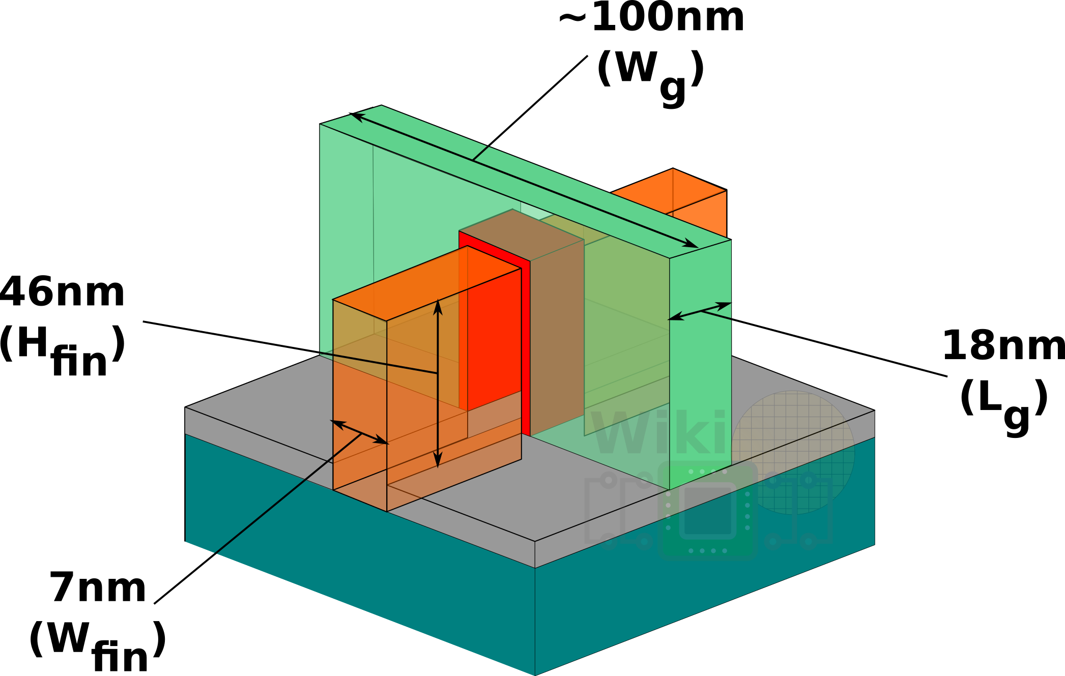
As far as cell size is concerned, there are no surprises. TechInsights silicon measurements matches Intel’s own IEDM paper. The metal pitch has shrunk from 52nm to 36nm and the gate pitch shrunk from 70nm to 54nm. They use contact-on-active gate (COAG) and have shrunk the cell height to 272 nanometers.
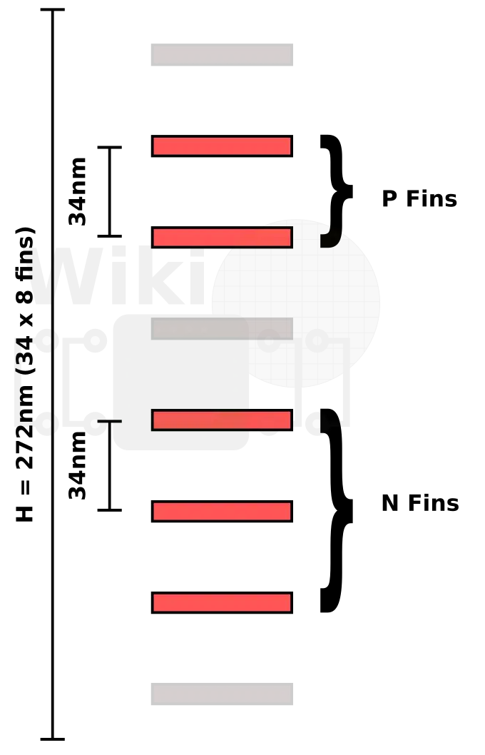
Since Intel has been using FinFETs for their 22, 14 and 10-nanometer processes, their standard cells are all fin-quantize. A standard cell is 272nm high and comprises eight diffusion lines. This is a reduction of 0.68x from the 399nm which consisted of 10 lines (actually 9.5 lines high, but based on 10 lines) which was a reduction from 14 lines at the 22nm node.
With eight diffusion lines, it means Intel can only pack 5 active fins. In other words, they are using 3 N fins and 2 P fins for their standard library.
If we were to design something like a NAND2 gate, then we would have two active gates and a single dummy gate at each of the cell boundaries. In other words, the width of the cell would be three gate pitches wide. TechInsights has measured a 54nm minimum gate pitch (identical to Intel’s IEDM paper), therefore the NAND2 cell width is 162 nanometers wide.
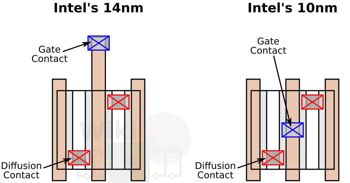
Intel’s first metal layer (M0) has a pitch of 40 nm. Techinsights has confirmed Intel is using contact-on-active gate (COAG). While the contact over the source-drain can be in the active region, the gate contact is traditionally dropped off the active region and over the isolation region. This is done to prevent shorting the gate. For their 10nm, Intel introduced the COAG process in order to allow the gate contact to be dropped right on top of the active gate, thereby further compaction the cell height.
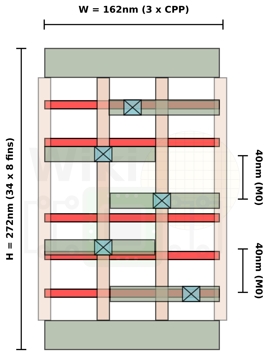
Continuing to build the cell from before, the M0 layer with a 40nm pitch now spans the cell with the COAG dropping down directly to the gate electrode below it.
The tightest pitches reported to date come from their Metal 1 layer with 36-nanometer pitches. Intel’s M1 is actually unusually dense, allowing for a great number of possible combinations of valid pin points to the M2 above. This is likely a key enabler for the efficient routing of their dense 10nm cells.
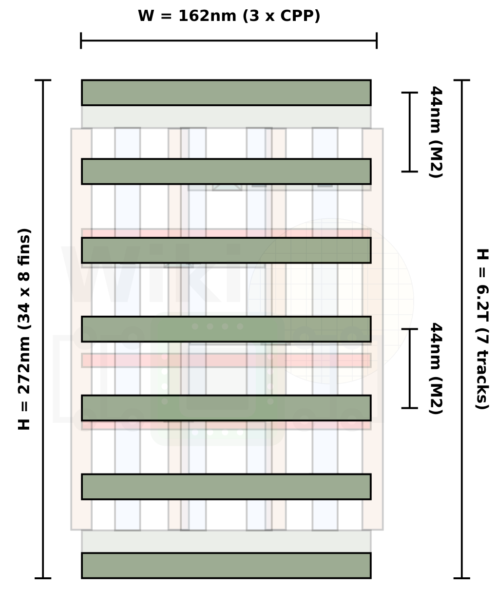
The Metal 2 track height measured by TechInsights is 6.2-Track high which also matches what Intel reported. With a cell height of 272nm and an M2 pitch of 44nm, there are 7 tracks which are shown below.
Density
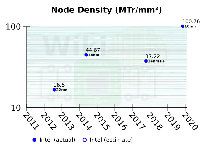
As far as density is concerned, the Core i3-8121U uses a process with a density, based on Intel’s metric, of 100.76 MTr/mm². This is a result of a transistor density of 90.78 MTr/mm² for packed NAND2 gates and 115.74 MTr/mm² for packed SSF cells.
Cobalt, Ruthenium
The minimum design rules for Intel’s 10nm are shown below. For the nitty-gritty stuff, check out our detailed article from IEDM. For the three lowest layers (poly, metal 0, and metal 1), Intel introduced Cobalt and Tungsten. What’s interesting though is that TechInsights also found Ruthenium along with Cobalt in the metallization stack. Intel has never mentioned using Ruthenium for their process at any of the conferences we have attended (including VLSI, ISSCC, and IEDM). However, this isn’t too surprising because in recent years Cobalt, Ruthenium, and Manganese were discussed by both Intel and Applied Materials as possible future metallization schemes. It’s worth noting that Samsung, IBM, and GlobalFoundries have also discussed Cobalt and Ruthenium for sub-7nm nodes in past conferences.
| Design Rules | |||
|---|---|---|---|
| Layer | Pitch (nm) | Metal | Patterning |
| Fin | 34 | SAQP | |
| Poly | 54 | with Co | SADP |
| Metal 0 | 40 | Co | SAQP |
| Metal 1 | 36 | Co | SAQP |
| Metal 2 | 44 | Cu | SADP |
| Metal 3 | 44 | Cu | SADP |
| Metal 4 | 44 | Cu | SADP |
| Metal 5 | 52 | Cu | SADP |
| Metal 6 | 84 | Cu | Single |
| Metal 7, 8 | 112 | Cu | Single |
| Metal 9, 10 | 160 | Cu | Single |
| Thick Metal 0 | 1,080 | Cu | Single |
| Thick Metal 1 | 11,000 | Cu | Single |
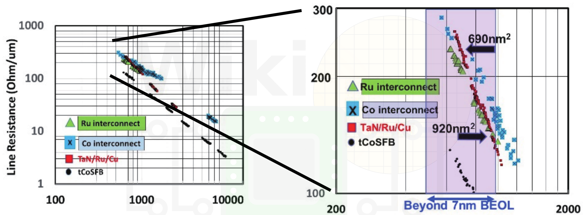
As a refresher, we want to point out that both Cobalt and Ruthenium are what’s called barrier-less conductors. They do not need barrier layers like Cu does that have stopped scaling (largely the effect of the industry reaching nanometer-thickness barriers, impacting integrity). Cobalt has shown superior EM and TDDB over copper at high-current low-cross-sectional wires which is one of the primary reasons Intel switched to Cobalt. What’s more interesting is, at last year’s VLSI Symposium, IBM/Globalfoundries reported that the thinnest possible Cu barriers can be achieved by using Cu with TaN/Ru barriers or tCoSFB (Through-Cobalt Self Forming Barrier). By the way, they also claim that Cu with tCoSFB has lower line R than even Co and Ru, meaning there is no cross-over point where Co would be better than Cu. But that seems to go against what Intel is doing with 10nm. It’s unclear who is right. So there is clearly a fork in the road as far as interconnects go.
We do not know exactly where Ru was found (the info is reserved for TechInsights subscribers) but given everything discussed, we suspect Intel is using Ru/Cu wires for their Metal 2, 3, and 4 layers. This is likely done for the exact reason GlobalFoundries reported – create the thinnest possible barrier. It will definitely be interesting to see what the rest of the industry converges on.
–
Spotted an error? Help us fix it! Simply select the problematic text and press Ctrl+Enter to notify us.
–