
TSMC N7+ EUV Process Starts Shipping
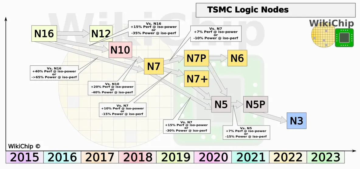
Today, TSMC is announcing that the company’s N7+ which has entered mass production the second quarter of this year is now delivering customer products to the market. N7+ is built on top of TSMC’s highly successful 7-nanometer process but introduces EUV technology on a few critical layers in order to reduce the design complexity.
TSMC is claiming that since it has begun volume production in the second quarter of 2019, it is matching yields to the original N7 process. We have recently covered TSMC’s roadmap which goes into a bit more details on TSMC N7 yield claims. In a press release, the company stated that “EUV tools have reached production maturity, with tool availability reaching target goals for high-volume production, and output power of greater than 250 watts for day-to-day operations.” Currently, TSMC is using the NXE:3400B with a reported power that greater than 250 W (presumably around 275 W) and we take it to mean that the consider the tool production-ready with availability exceeding 90%. Those values are similar to what Anthony Yen from ASML reported earlier this year. The N7+ process is currently used by Huawei for select products and is expected to be leveraged by AMD for their Zen 3 microarchitecture.
Looking a bit further, TSMC will introduce N6 into risk production in the first quarter of 2020 and volume production by the end of the year. N6, like N7+ will improve density by around 20% but will use design rules fully compatible with N7 which is where we expect most customers to migrate to eventually. N6 ramp will coincide with the mass production of the company’s next major node, the 5-nanometer process.
–
Spotted an error? Help us fix it! Simply select the problematic text and press Ctrl+Enter to notify us.
–