
Analog AI Startup Mythic To Compute And Scale In Flash
When it comes to AI hardware, no stone is left unturned. One company WikiChip has been watching closely is Mythic. That company hasn’t fully lifted the lid on their architecture and products but some details have started to trickle out. At the recent AI Hardware Summit, the company’s founder and CEO, Mike Henry, gave an update on the chip.
Founded in 2012 by Mike Henry and Dave Fick, the Austin-based startup recently finished raising $70 million in Series B funding, bringing the total amount raised to just over $85 million. Today, the company has grown to 110 employees.
Mythic is an analog company. But before we touch on the details, it’s important to point out that they are currently focused on inference only – both at the data center and at the edge. The two markets are expected to reach a TAM of $25 billion by 2024 which is why there is so much focus here. Longer-term, Mythic plans to target the mass-market consumer and automotive products.
Keep Everything On-Chip, In Flash
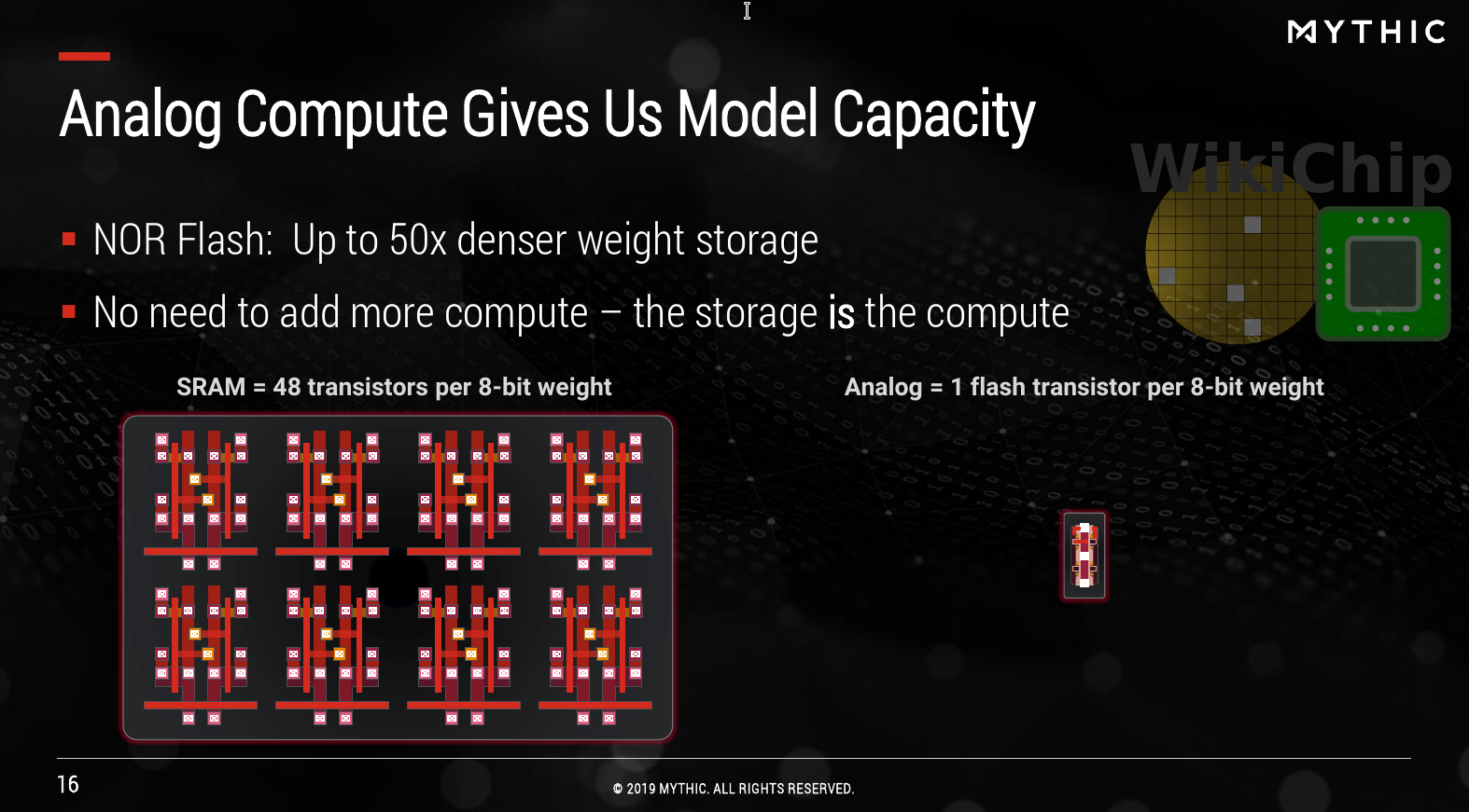
As the accuracy of models improves, so does their size. Today, models reach 100s of millions of parameters and even into the billions. On top of that, there is the demand for deterministic behavior such as consistent frame rate and latency – often in real-time. And this is where Mythic comes into the picture. Mythic’s thesis is simple: pack enough storage on-chip along with a ton of parallel compute units in order to maximize the memory bandwidth and reduce the power of data movement. But there’s a twist – and this is where Mythic’s original approach shines – the company ditches traditional SRAM for much denser flash cells and on top of that, Mythic plans on doing the compute natively in analog, directly in-memory.
But why flash? The answer is really simple: because it’s dense, low power, and cheaper, almost two whole orders of magnitude denser than SRAM.
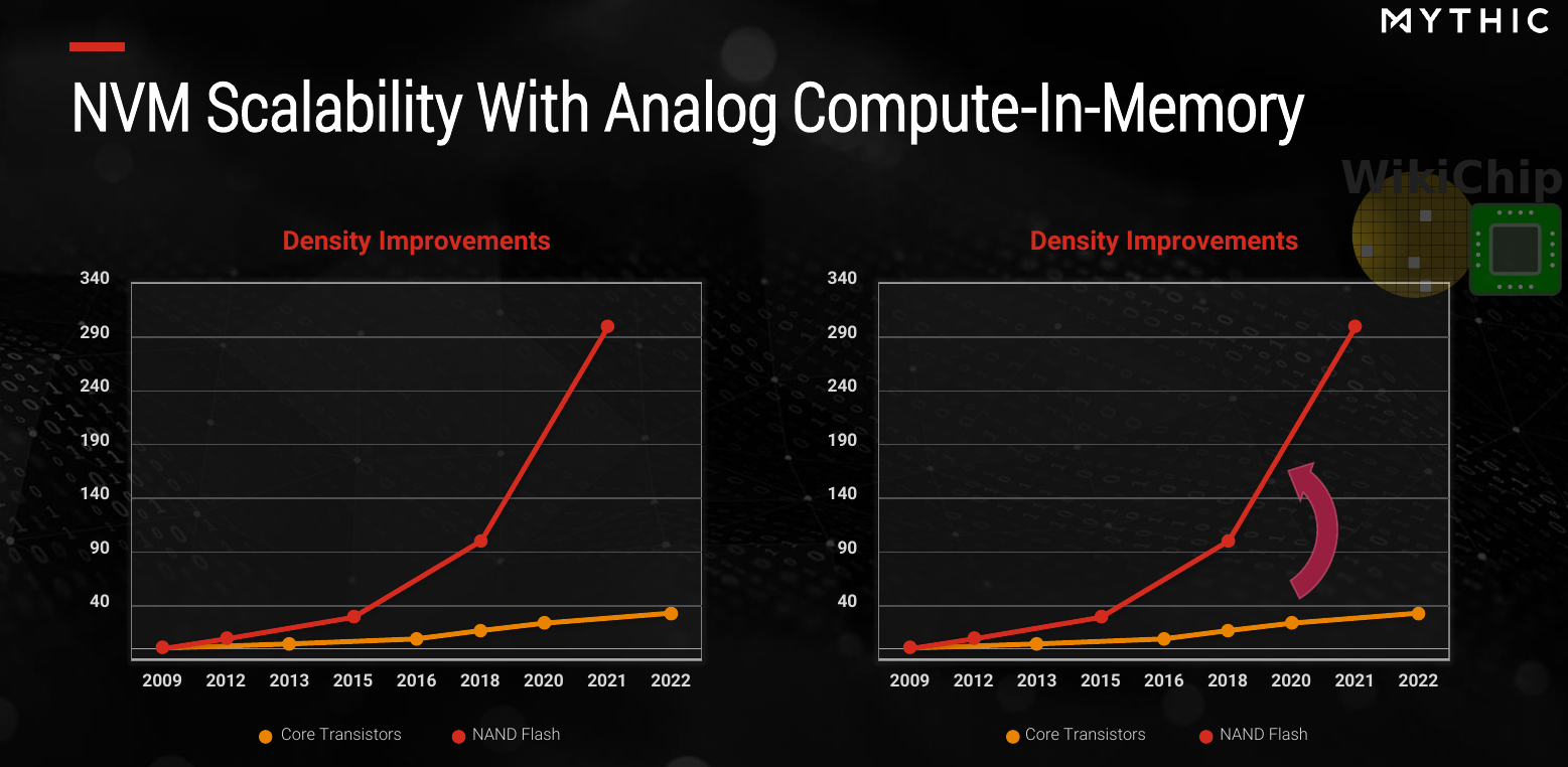
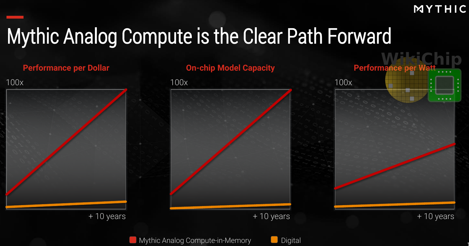
Mythic’s chips, in theory, scale more like memory rather than traditional CMOS. When looking at the longer roadmap, the benefits are more profound as SRAM bitcell scaling is getting ever more difficult. Across the board – in terms of performance per dollar, density per unit cost, and performance per watt – this is a potentially big win.
We have seen a whole bunch of roadmaps over the years and it’s easy to dismiss it when they start talking about 10 years out. But for Mythic, there are a few things different. In particular, it’s worth pointing out that currently, Mythic is working on embedded flash in a 40-nanometer process. They have a fairly clear path to 28 nm and 22 nm, therefore loosely speaking, half-way into that graph is predicated on existing nodes that are already shipping today. Mythic’s CEO, Mike Henry seems convinced they can continue this further but while there is some work being done to continue scaling to the 16/14-nanometer nodes, it’s unclear if this will come to market. Many in the industry believe that embedded flash hit the wall at 22 nm. In a brief talk with Mythic, they told us that they are not married to embedded flash and that if one of the emerging technologies (e.g., multi-bit ReRAM, PCM, or NRAM) emerges as a strong alternative, they would certainly consider migrating to such technology.
IPU
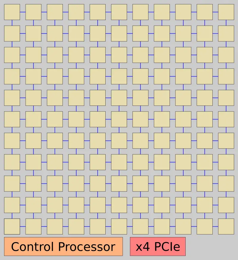
Mythic’s chips are called IPUs or Intelligence Processing Units. In terms of peripherals, the chip is very simple, consisting of x4 lanes of PCIe, a basic control processor which is responsible for the management of the entire chip, and the DNN tiled grid. Since the chip is designed to store the entire model, there is no DRAM.
Mythic stated that since this is a tile-based design, they could add further customization by adding direct audio/video and various other interfaces if there is demand. At last year’s Hot Chip, Mythic was talking about an initial product with 50 million weights. At the recent AI Hardware Summit, Mike Henry stated that initial products will have up to 120 million weights which is quite a bit more than originally planned. On the Fujitsu 40 nm process, a near-reticle full-size die should have a capacity of around 300M weights, so 120M is still a fairly big die.
The IPU is intended to serve as a PCIe accelerator connected to a host. For large models or multiple models, multiple IPUs can be used. Models are initially loaded onto the IPU where they remain stationary. There is no DRAM and programming flash is relatively slow therefore the models should be able to fit into the chip with multiple applications mapped onto the same chip. This is fairly typical for many edge applications. Under normal operation, the host CPU will send the data to the IPU and receive the result back over the PCIe port.
The chip comprises a grid of DNN tiles. Inside a tile is the analog matrix multipliers built on top of a large pool of embedded flash memory for weights. An embedded flash cell uses a floating gate to store a bit by storing a charge, manipulating the threshold voltage. The transistor supports 256 levels of conductance (G = 1/R) between the fully off and on states which Mythic uses to represent 8-bit values.
By mapping all the neuron weights onto the flash transistors, they can use Ohm’s Law to naturally perform matrix multiplication operations. The way this is done is by using the flash transistors to represent the weights as a variable resistor. This is performed once prior to the calculations. Using 8-bit DACs, the input vector is applied as a set of voltages across the variable resistors. Using Ohm’s Law, the output current is the result of the multiplication of the input data and the weights vectors (I = V x G). The accumulate is done by wiring columns of resistors. Finally, a set of ADCs turns the resulting current back into digital values which becomes the output vector. The ReLu and various other non-linear operations are done by the ADCs at that point as well.
There is some additional logic around this component. The DAC/ADC wrapper does compensation and calibration in order to get accurate 8-bit computation regardless of the operating conditions – similar to what’s done with image sensors today.
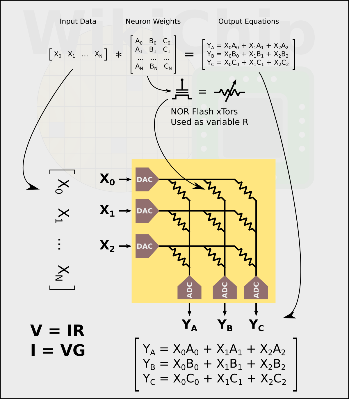
Some things to point out about this scheme is that there are no actual memory accesses. The matrix multiply themselves are done in-memory, leveraging Ohm’s Law, so there is no weight access energy. With stationary weights, there are also no batch sizes or other special handling. Though the fixed capacity might pose some problems. By the way, they support neuron sparsity but not weight sparsity.
Interestingly, Mythic says that for their first-generation, in order to speed up the development and time-to-market, they won’t be using DACs for the inputs. Instead, they are using a digital approximation circuit whereby each input bit is computed separately and then accumulates the results. This is something that they will be eliminating with DACs in the future which is expected to provide them with some nice improvement.
–
Spotted an error? Help us fix it! Simply select the problematic text and press Ctrl+Enter to notify us.
–