
AMD 3D Stacks SRAM Bumplessly
Last week Computex Taipei 2021 was held virtually. While the event was largely a hit or miss among the chip vendors, one of the more interesting announcements that were delivered at the event was AMD’s 3D V-Cache – a 3D stacked SRAM. But while the stacked SRAM is interesting enough, the real announcement was the introduction of DBI into mass production in their highest-end chips by next year.
3D V-Cache
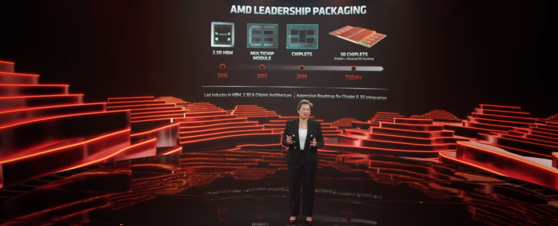
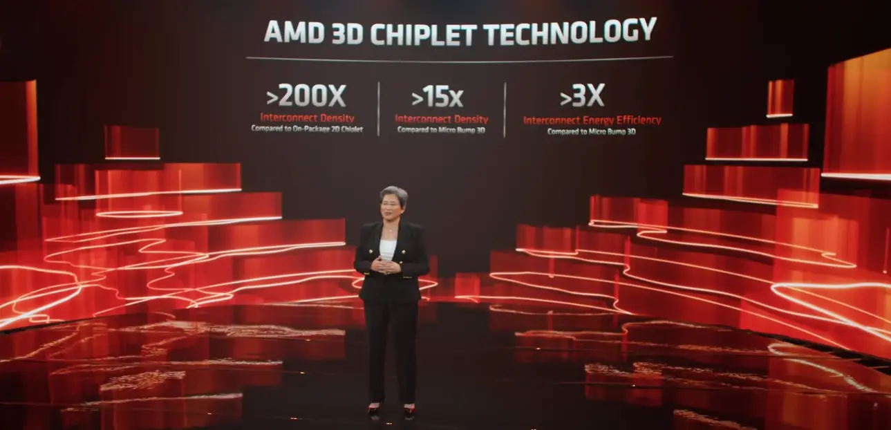
At the closing portion of the AMD event, AMD president and chief executive officer, Dr. Lisa Su went onto talking about some of the advanced technologies the company is working on. AMD disclosed their first application of true 3D chiplet stacking they called “3D V-Cache”.
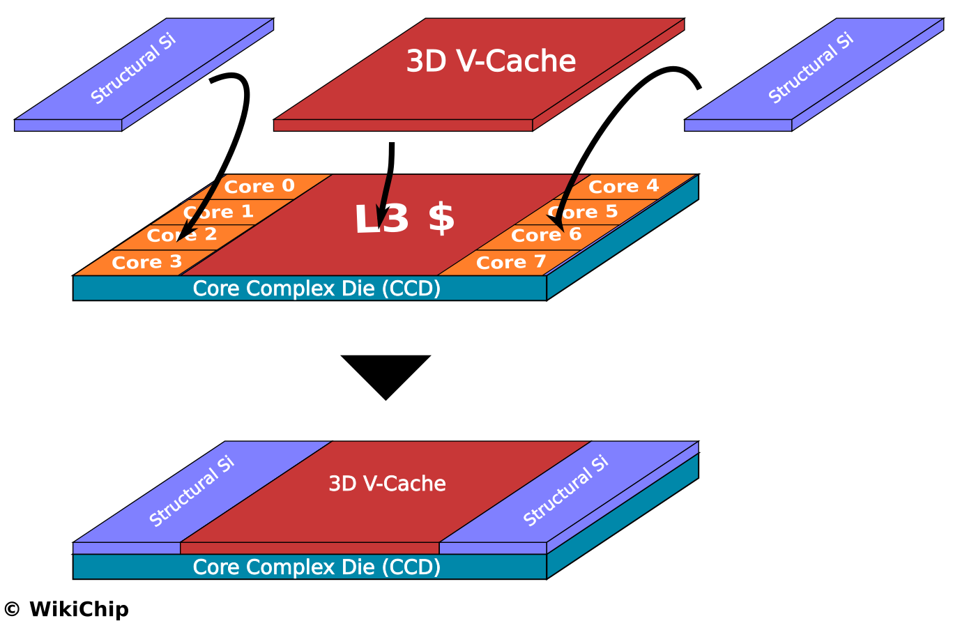
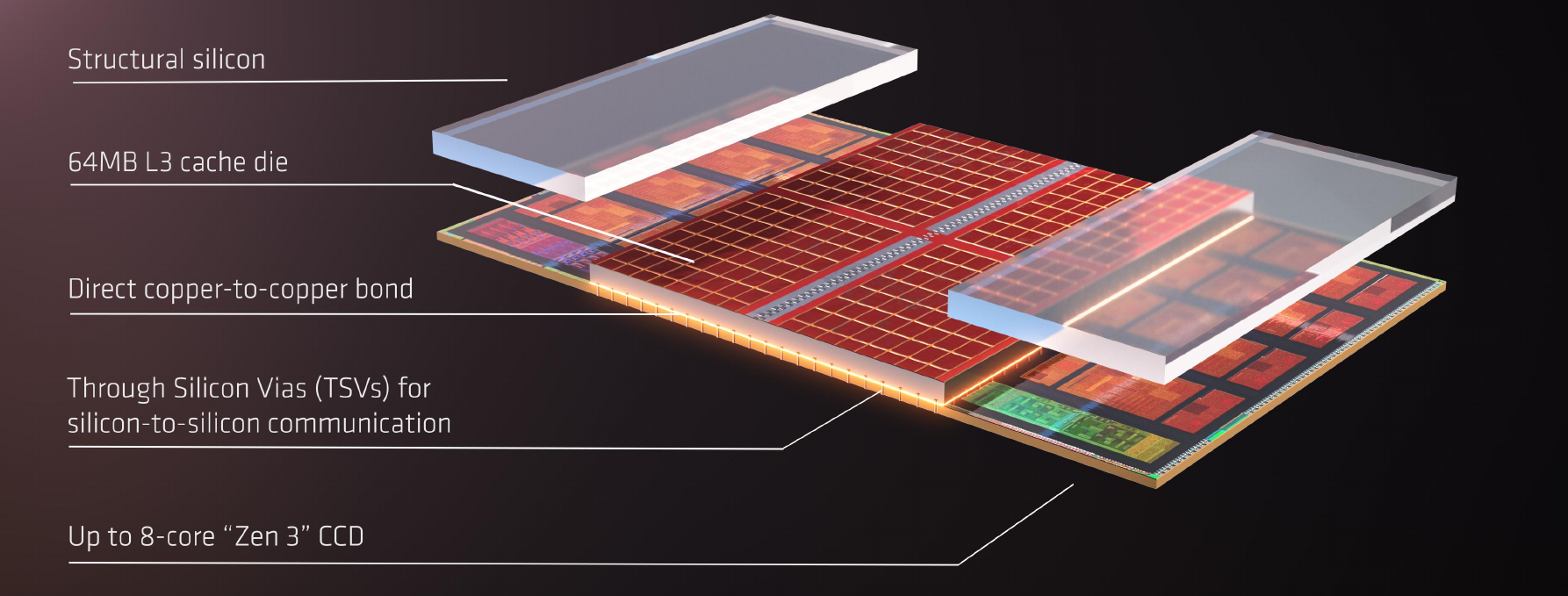
A prototype chip was also shown at the event. AMD showed a Ryzen 5000-series microprocessor that incorporated the V-Cache. The Ryzen 5000-series microprocessors incorporate one or two Core Complex Dies (CCDs) along with an I/O Die (IOD). The V-Cache is a 64 MiB SRAM die that is said to be fabricated on TSMC’s 7-nanometer process. The V-Cache die is thinned and is then stacked directly on top of each CCD directly above the existing L3 cache area. On the Ryzen 5000-series microprocessors, each CCD features 32 MiB of L3 cache, therefore the V-Cache effectively triples the L3 capacity of each CPU. Two additional structural dies are added on top of the CCDs above the CPU complex. It’s unknown if those structural dies are blank silicon or if they include anything special (e.g., inactive thick copper traces which can enhance the thermal conductivity of the dummy die).
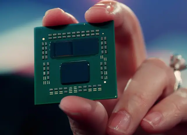
Below is a photo of Dr. Su holding a prototype chip with the left CCD exposed, showing the SRAM die.
The 64 MiB 3D V-Cache die itself is measured 36 mm² (a 6 mm x 6 mm square). This is roughly 9 mm² more than the 32 MiB of L3 on the CCD which occupies around 27 mm² of silicon so the SRAM in the 3D V-Cache appears to be more tightly packed. Architecturally, the V-Cache die itself adds 64 MiB of SRAM capacity directly on top of the existing 32 MiB of L3 for a single, large, 96 MiB of L3 capacity. A complete chip with two CCDs would therefore have a maximum L3 capacity of 192 MiB per processor. The L3 bandwidth is said to be tripled to 2 TB/second while maintaining the same latency.
DBI Commercialization in High-Performance Logic
While the stacked SRAM is interesting, the bigger news appears to be the move to direct bond interconnect, or DBI. DBI or Hybrid Bonding is a permanent bond of the embedded copper interconnects directly without bumps or pillars. This isn’t the first time DBI has been used (Sony, for example, first used it in the IMX260 which was used in the Samsung Galaxy S7 back in 2016), but this would appear to be the first time it’s used in high-performance logic applications.
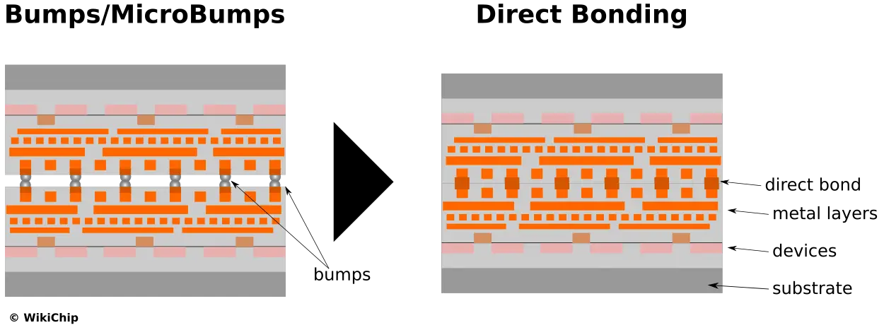
As part of the 3D V-Cache disclosure, Dr. Su went on to disclose some additional key technologies involved here. “We are using a hybrid bond approach with through-silicon via that provides over 200-times the interconnect density of 2D chiplets and more than 15 times the density compared to other 3D stacking solutions. This actually enables much more efficient and denser integration of our IP,” Dr. Su said.
Note that the >200x interconnect density refers to “on-package 2D chiplet” (presumably standard MCP). The slide that was shown at the time specifically said “compared to micro bump 3D” when she referred to “other 3D stacking solutions” for both density and energy. “The die-to-die interface is using a direct copper-to-copper bond with no solder bumps of any kind. This approach dramatically improves the thermals, the transistor density, and interconnect pitch and is only one-third the energy-per-signal of micro bumps 3D approaches,” she added. “All of these things make this truly the most advanced and flexible active-on-active silicon stacking technology in the world.”
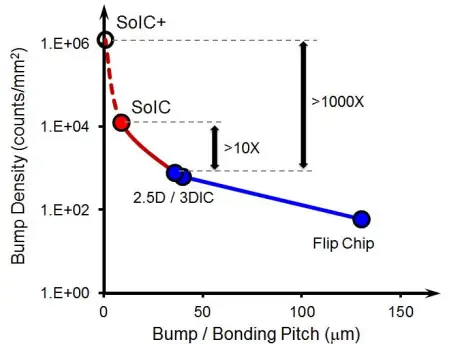
On a typical MCP such as the one AMD uses, we’re looking at as much as 100 bumps/mm² or so. By comparison, Intel’s current generation of Foveros – such as that found in Lakefield – uses 50 um pitch micro-bumps which yields a density of roughly 400 connections/mm². 15 times the density compared to the current Foveros generation implies around >6,000 connections/mm². TSMC reported a bond pitch in excess of 10,000 for their SoIC so this seems about where you’d expect the first-generation DBI to be. Hybrid bonding smaller than 10-micron can far exceed 10,000 connections (e.g., Sony already exceeds 4-micron pitch in 2019 on their image sensors). Intel advertised their power for Lakefield at around 0.15 pJ/bit. V-Cache connections would be at around 0.05 pJ/bit or about a third. It’s worth pointing out that Intels’ Foveros does have a series of future generations including micro-bumps down to 25-micron (and density exceeding 1600 connections/mm²) as well as various 10-micron and below direct bond implementations similar to TSMC’s, albeit no product has yet been announced to utilize those technologies. Other companies such as GlobalFoundries have also announced hybrid bonding technologies.
| Advanced Packaging Technologies | |||||||
|---|---|---|---|---|---|---|---|
| Intel | TSMC | ||||||
| Tech | HBM | EMIB | EMIB (Future) |
Foveros | Foveros (Future) |
Foveros (Future2) |
SoIC |
| Bond | Micro-Bumps | Hybrid Bonding | |||||
| Pitch (µm) | 55 | 55 | 36 | 50 | 25 | ≤ 10 | ≤ 15 |
| Density (wires/mm²) |
350 | 350 | 750 | 400 | 1,600 | ≥ 10,000 | ≥ 8,000 |
SoIC

The disclosed information implies AMD will be utilizing TSMC’s System on Integrated Chips (SoIC) technology. SoIC is an umbrella brand term used by TSMC to describe a whole set of back-end 3D stacking packaging technologies which, in turn, can be holistically integrated into any other front-end technology such as flip-chip (as in the case of AMD), CoWoS, or InFO. A special characteristic of SoIC is its highly dense bonding pitch reaching sub-10 μm.
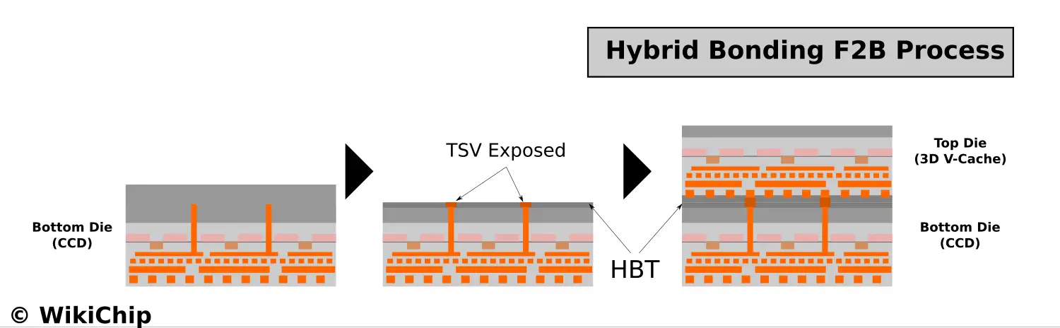
When 3D stacking, chiplets are interconnected either face-to-face or face-to-back (or both). If we assume the Ryzen 5000-series package used is largely unchanged, this implies they are using a face-to-back bonding flow (with the CCDs facing down as usual). Dr. Su did note that they are using Hybrid Bonding with TSVs which implies this is, in fact, a F2B process. Under this process flow, you’d have the CCD wafer mounted on a carrier that is thinned down to expose the TSVs from the backside. The hybrid bond terminal is then formed on the back side. The 3D V-Cache die is also thinned and is then attached face-down.
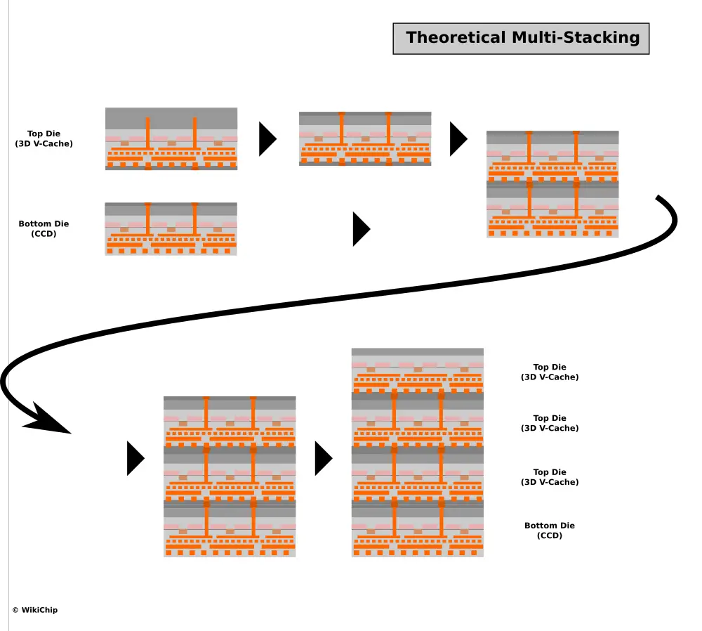
An interesting consequence of using a F2B flow – as opposed to a face-to-face flow – is the fact that this process flow is actually repeatable. In other words, the 3D V-Cache itself can also be thinned down to expose its own TSVs from the back-side, allowing another 3D V-Cache die to then be attached face-down on top of it. This is somewhat similar to stacked HBM in spirit, but the packaging technology is obviously very different. It would also require the underlying logic implementation to support such a design. Note that currently, AMD is only talking about a single 3D V-Cache stacked. Nonetheless, the possibility is there.
Production By EOY
AMD said they expect to start production by the end of the year. AMD didn’t reveal which products will utilize the new technology other than to say that it’s their highest-end products. Production starting by the end of this year implies we can expect to see the tech in products in early 2022.
–
Spotted an error? Help us fix it! Simply select the problematic text and press Ctrl+Enter to notify us.
–