
Samsung 7nm Enters Risk Production, Talks Roadmap, Scaling Boosters, and the ARM Ecosystem
It has been a little over a year since Samsung split off its foundry business in a bid to capture 25 percent of the foundry market share within five years. During that time, they have been executing on their aggressive process technology roadmap, including attempting to bring the first EUV process to mass production. Last week Samsung held their annual Samsung Tech Day which happened to coincide with ARM TechCon. Luckily Samsung held a number of sessions at TechCon talking about their foundry business along with their future plans.
Core Tech
Process technology is their core competency. Currently, this is split into two main branches: a mainstream path based on their standard CMOS FinFET technology and a differentiation path based on their FD-SOI technology for low power and IoT applications.
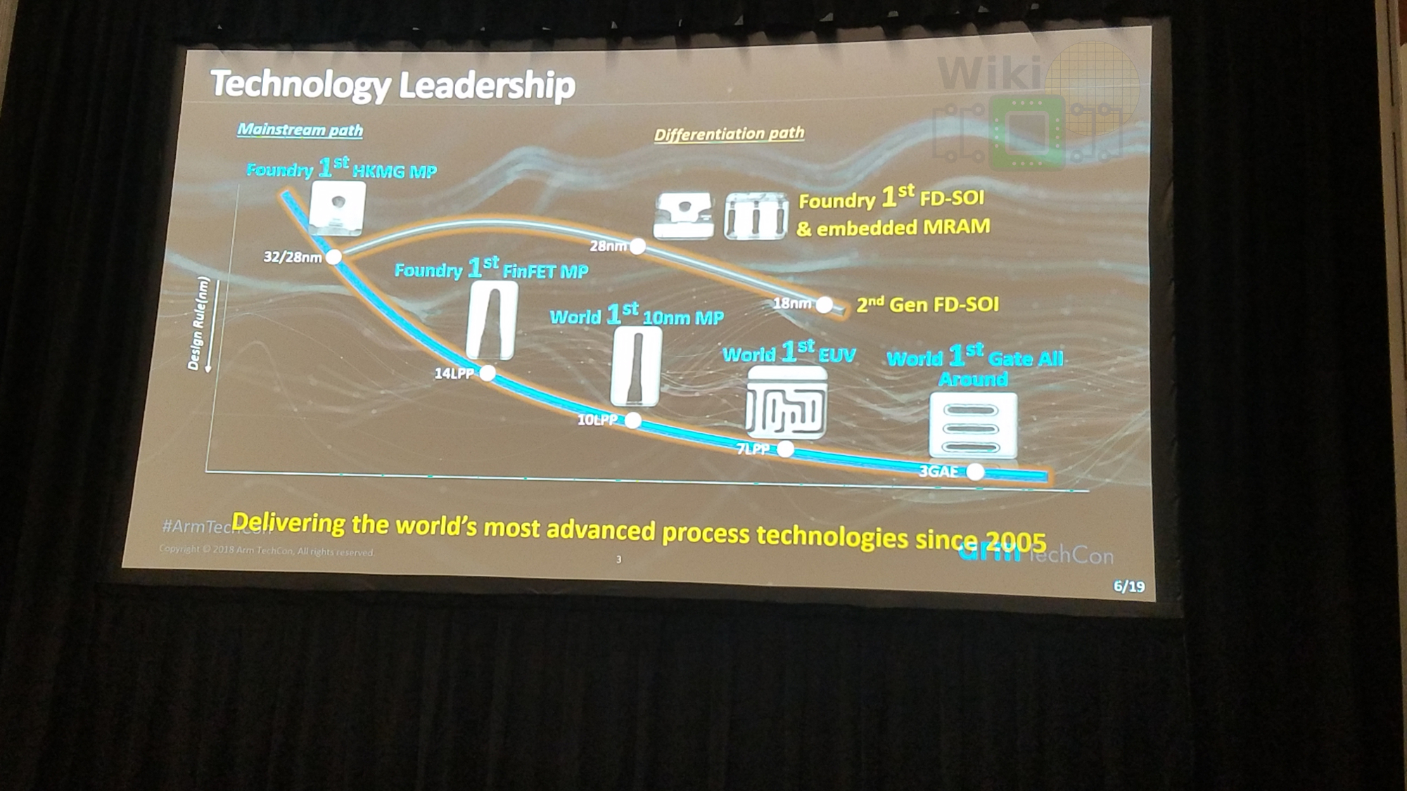
Augmenting their 28nm FD-SOI is their new embedded MRAM offering. Samsung says they have test chips made with the technology and NXP has plans to utilize eMRAM for their products. 18FDS, Samsung’s next-generation FD-SOI node, is also fully defined but no timeline was disclosed for when we can expect those technologies to enter production. While 28FDS uses single patterning with a 90 nm metal pitch, 18FDS metal pitch is reduced to 64 nm, making use of double patterning.
For the mainstream path, there is very good visibility for Samsung for the next couple of years. Going horizontally across the roadmap, within each of the blue rectangles there is strong design rule compatibility that starts at the light blue square which Samsung calls “Innovation Nodes” and continues with a series of sub-nodes which incorporates incremental improvements. At each of those innovation nodes, Samsung introduces new technologies (e.g., EUV, GAA). At each of the sub-nodes, called “Evolution Nodes”, Samsung introduces incremental changes that largely build on the prior node with some technologies borrowed from other future nodes. The key takeaway is that evolution nodes provide a relatively frictionless migration path which allows for IP reuse while introducing PPA improvements.
In their 14 nm class, the 11LPP node brings the final set of improvements including a new ultra-high density cell. It is by far the best ‘bang for your buck node’ and Samsung expects it to be a long-lived node. On ARM’s side, additional products for the automotive industry including safety packages (incl. FMEDA reports, etc..) were introduced with design kits already available for designers.
Likewise, the 8LPP node is a backward-compatible extension to their 10 nm node which brings a light pitch shrink. 8LPP was designed to offer a low-risk migration path forward while progress was being made on their 7 nm EUV process. Recently Samsung introduced another enhancement called 8LPU which has the same design rules as 8LPP but has improved device performance, bringing it closer to 7LPP. In other words, 8LPU is Samsung’s most advanced non-EUV process node.
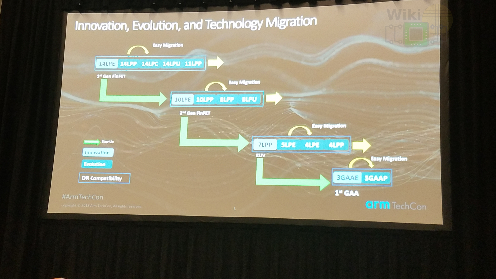
If you have been following Samsung’s roadmap closely you may remember that last year they had 5LPP with 4GAA following it. 5LPP and 4GAA have since been removed and 4LPE, as well as 4LPP, were added. The reason for this is simple. Samsung says they can reach the performance targets they were aiming at for 4 nm using FinFET without changing the device architecture to a GAA.
7LPP Update
The biggest news from Wednesday at 3 PM was the announcement that 7LPP has entered risk production and is expected to ramp throughout 2019. It’s expected that Samsung will be the first EUV-based process to enter mass production, although when and how high-volume it will be next year is still uncertain. Both Qualcomm and Nvidia have products planned for this process.

The announcement came earlier than anticipated due to an unexpected partner announcement. Samsung initially expected to reach this milestone around December but better than predicted improvements allowed them to move the timeline slightly forward. In the slide above, the yellow ‘ready for production’ line is the magic number of 1,500 WPD for the NXE3400 they have installed at S3 line in Hwaseong, South Korea. This is using a 250 Watt power source which the company says they have been steadily using for over six months now. Recently they have also demonstrated the ability to run at 280 Watts. S3 exclusive EUV line will complete by the end of 2019 with full-scale mass production scheduled for 2020.
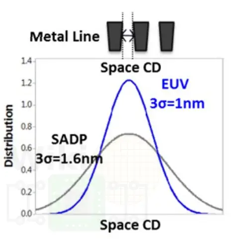
The 1,500 WPD reaffirms the fact that Samsung uses very high dosage (seems around 55 mJ/cm²) which is twice as much as what ASML normally quotes which is why Samsung is not getting anywhere near the 125 WPH that ASML mentions. On top of this, they are not using EUV pellicles which currently have a transmissivity in the high 70%s which would further reduce the throughput.
Going from 7LPP to 5LPE, there is no geometry change. The difference is largely in the standard library. In addition to a track reduction, Samsung re-introduces their single dummy gate. Based on Samsung’s description, we now believe that the 2nd-Generation 7nm process we covered from VLSI Symposium is more likely their 5LPE. We have adjusted our density plot below to reflect this. One thing we want to point out is that the slide above says “up to 40% area reduction”, but verbally they said “48%”. Both values imply that the MxP is more relaxed than the 36nm they quoted (or alternatively, the 36nm MxP is 5LPE). For 7LPP it’s quite possibly ≥ 40 nm. Nonetheless, we currently have no way of confirming this.
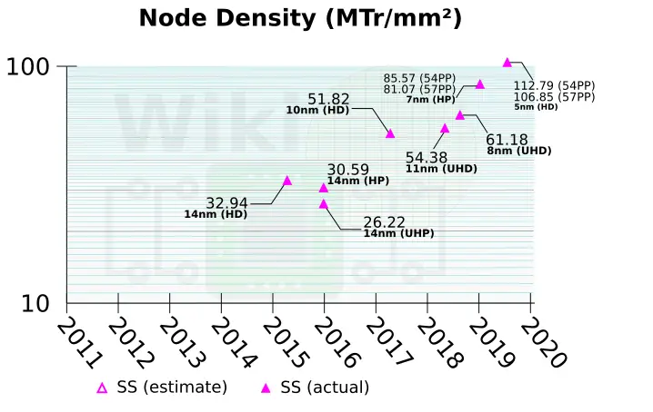
Samsung expects to start production of 5nm sometimes by summer next year with 4nm following shortly after. PDKs for those nodes will become available by the end of this year.
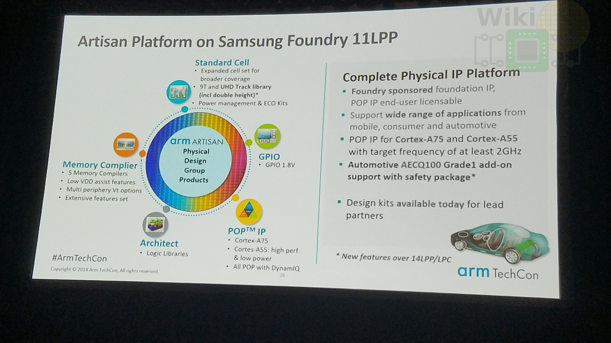
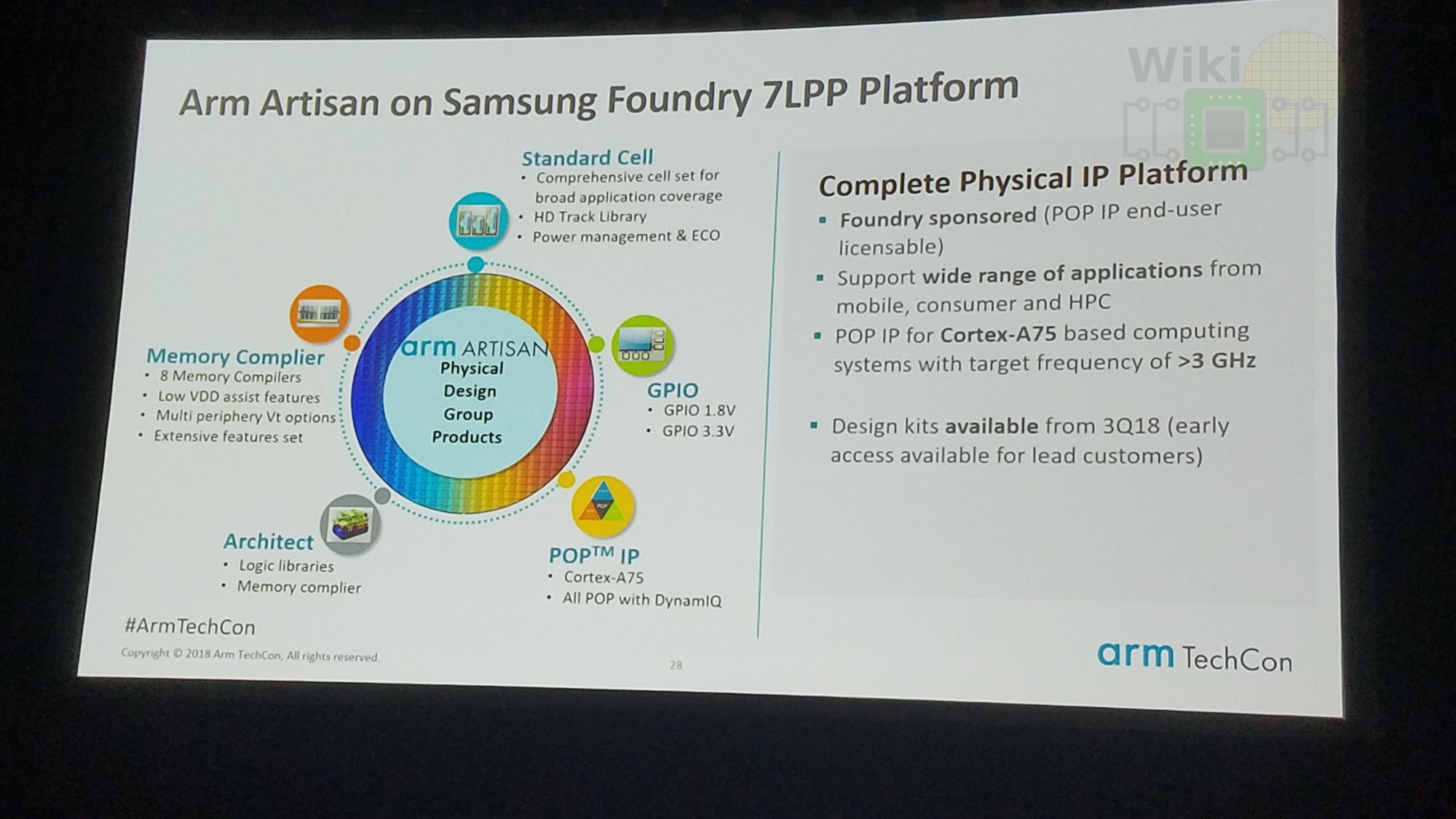
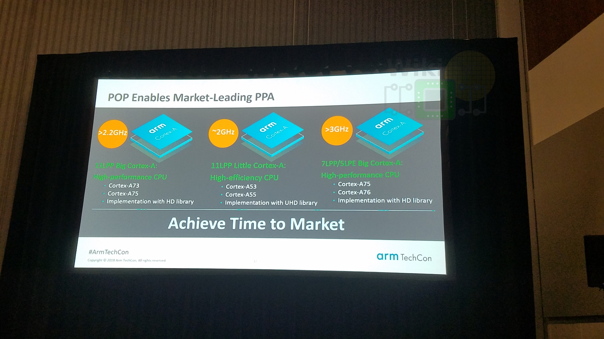
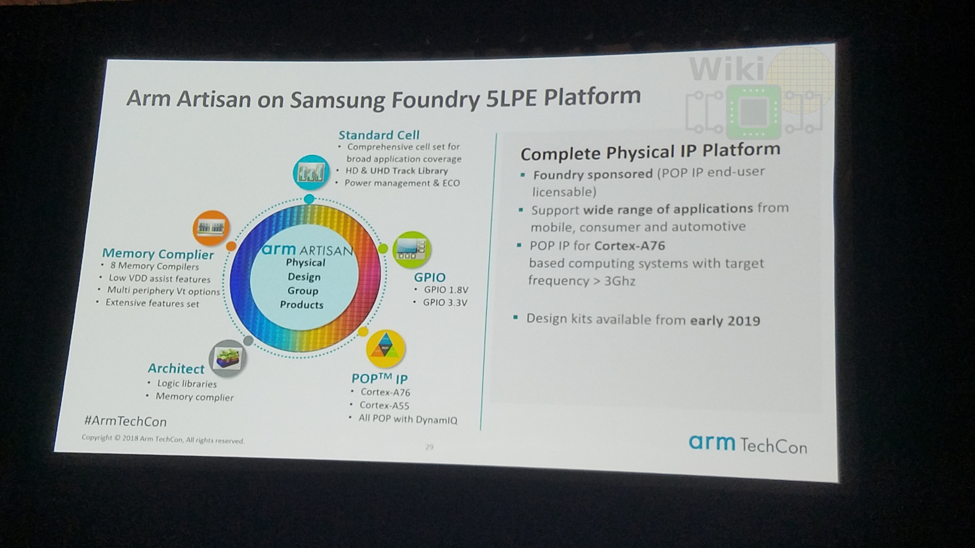
On Arm’s side, there is extensive platform support for 7LPP extending from mobile to HPC. Design kits are available as of today. Arm reported silicon based on their POP IP for the Cortex-A75 achieving target frequencies greater than 3 GHz.
Scaling Boosters
Samsung reiterated a number of scaling boosters they have integrated into their 7, 5, and 4-nanometer process nodes.
- Single diffusion break (SDB)
- Special cross-coupling structures
- Flexible contact placement
- Mixed diffusion break (MDB)
In addition to the standard gate pitch and metal pitch scaling, Samsung was the first to introduce single diffusion break with their 14nm process. Although 7LPP uses DDB, SDB was brought back with 5LPE. One of the new boosters we previously detailed is the special cross-couple constructs that allows for 45-degree routing.
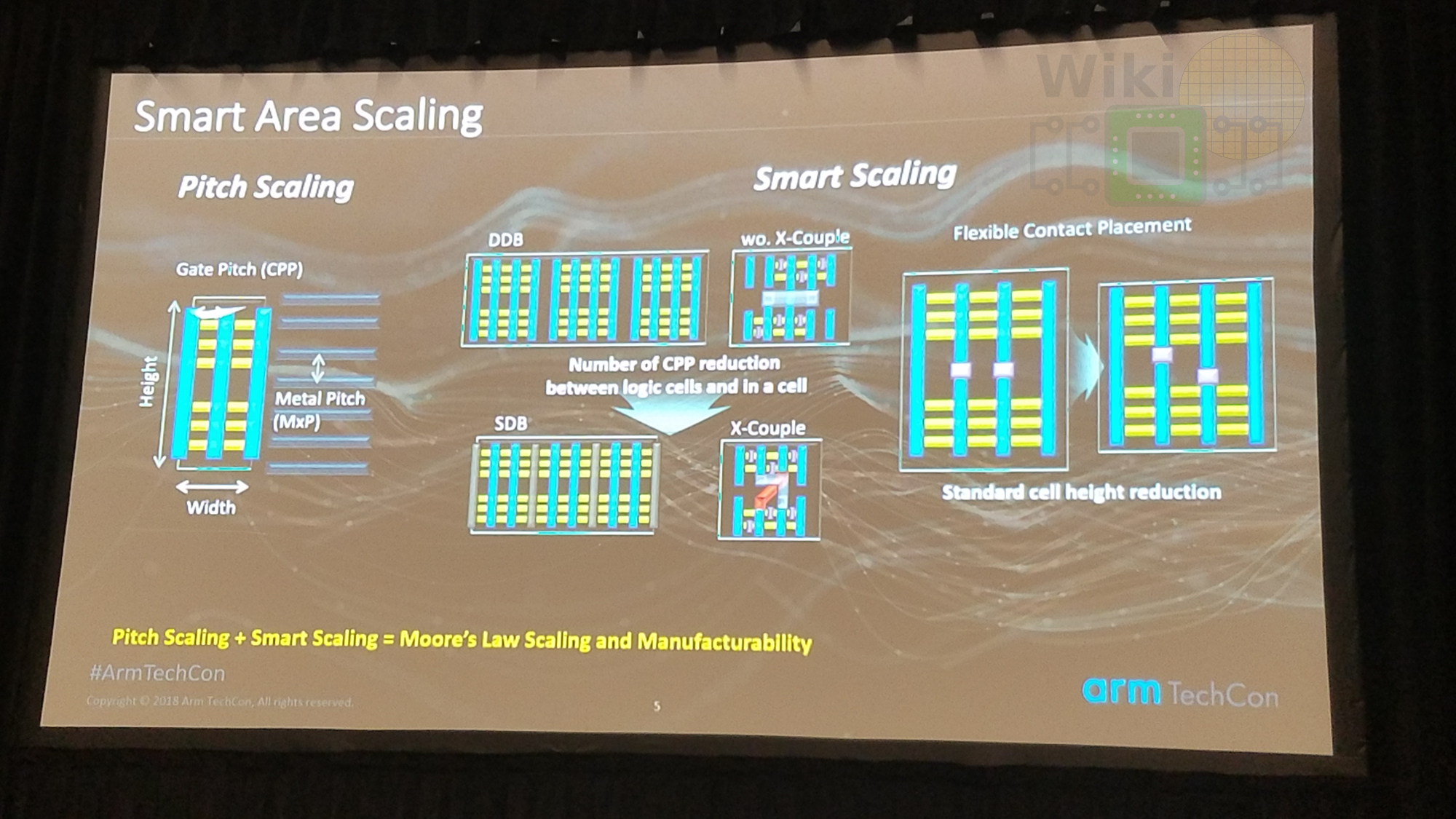
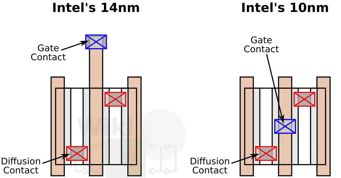
The flexible contact placement, which is being introduced with their 4nm node, is particularly interesting due to the problems it has given Intel with their 10nm. Samsung noted that this is very challenging which is why they are introducing it in stages. Initially, Samsung plans to allow the contact placement to shift from the isolation region to the edge of the diffusion region. Once this enters mass production and good yields are achieved, they will shift the contact further – over the active region.
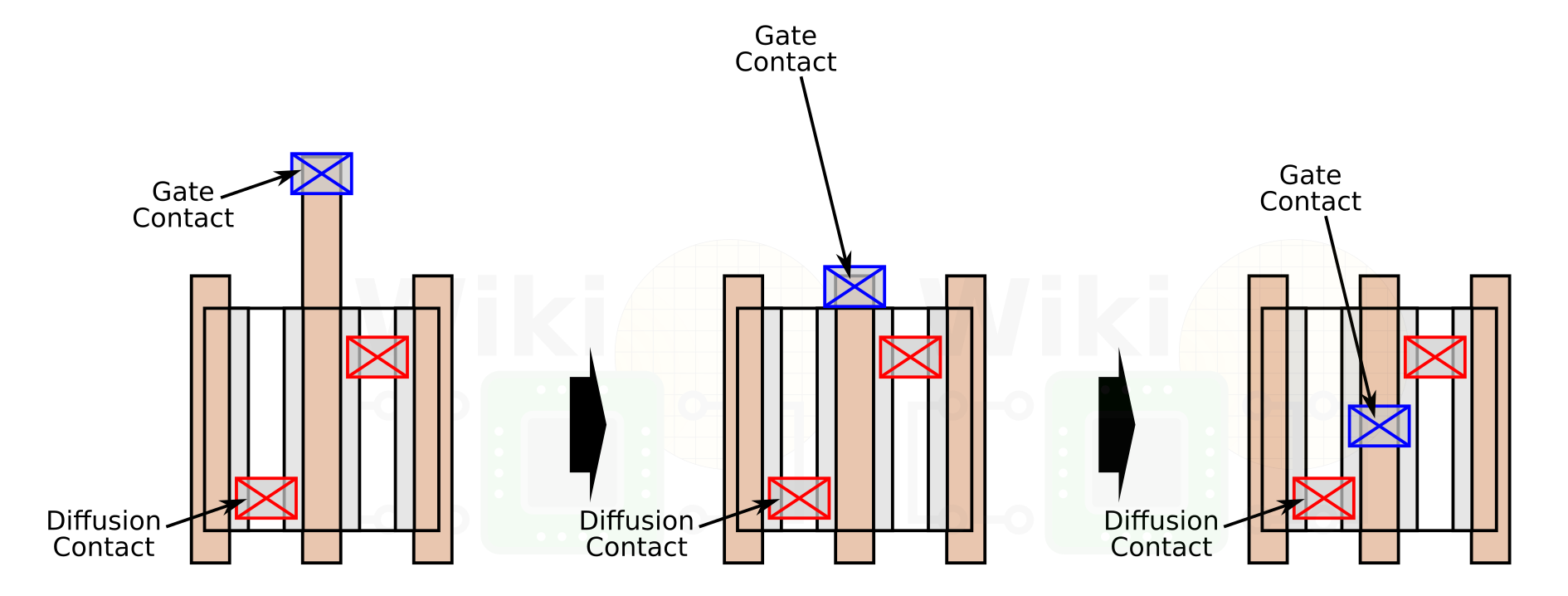
Intel has been trying to introduce this technique in their 10nm process for a while now. Unlike Samsung, Intel did not try to integrate COAG in a number of small stages, making yield learning considerably more complex. With that respect, Samsung’s approach is much more sensible and advantageous.
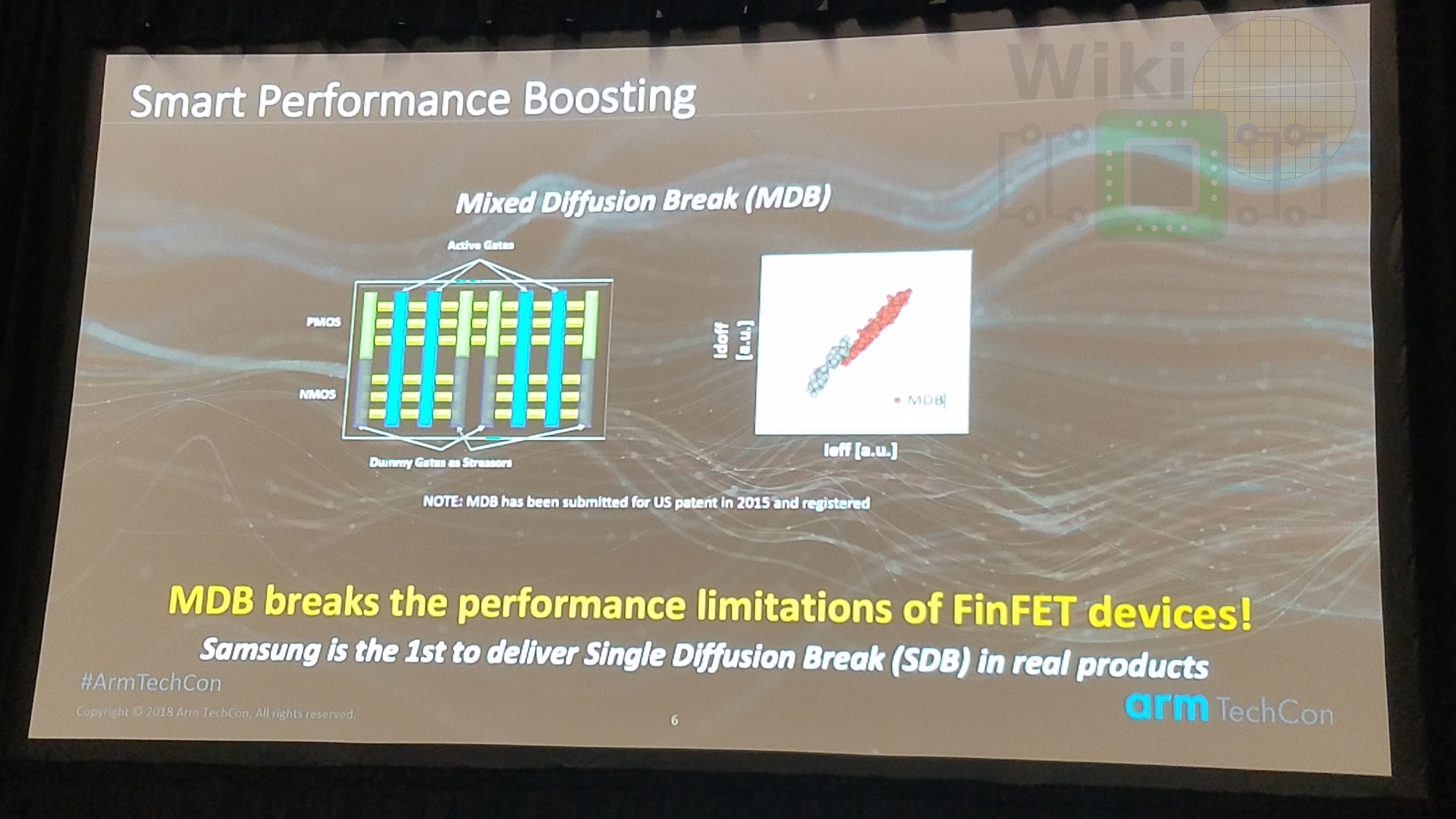
The last enhancement Samsung is introducing is mixed diffusion break (MDB). Since pMOS lags behind nMOS in terms of performance, with MDB, Samsung can allow pMOS to have a single diffusion break while nMOS can have double diffusion breaks, allowing lines to extend where wanted and dummy gates to serve as stressors elsewhere. This improves the area scaling while improving the performance. In the slide below Samsung has an Idoff vs Ieff graph showing improvement to both.
4nm appears to have reduced the MMP to 27 nm and the poly pitch down to 40 nm. This will be Samsung’s last FinFET process before moving over to a new device.
On Arm’s side, most of the 7LPP platform carries forward to 5LPE. Design kits will be available from Q2 2019. Arm reports targeting frequencies greater than 3 GHz for the POP IP for the Cortex-A76 for 5 LPE.
–
Spotted an error? Help us fix it! Simply select the problematic text and press Ctrl+Enter to notify us.
–