
Samsung Ramps 7nm, Preps 5nm, And Adds 6nm
Today Samsung is reporting a number of updates regarding their process technology roadmap.
Last year, the company’s EUV-based 7-nanometer node entered risk production. Today, Samsung is reporting that 7-nanometer has entered mass production.
5 nm
Samsung is also announcing that its development of the 5-nanometer FinFET process technology is complete and is ready for customers’ samples. The 5 nm node is said to provide up to 20% lower power at a constant performance or up to 10% higher performance at constant power compared to their 7 nm node.
| Samsung 5-nanometer Perf Claims | |||
|---|---|---|---|
| 14 nm vs 28 nm | 10 nm vs 14 nm | 7 nm vs 10 nm | 5 nm vs 7nm |
| -60% Power or +40% Perf | -40% Power or +27% Perf | -35% Power or +20% Perf | -20% Power or +10% Perf |
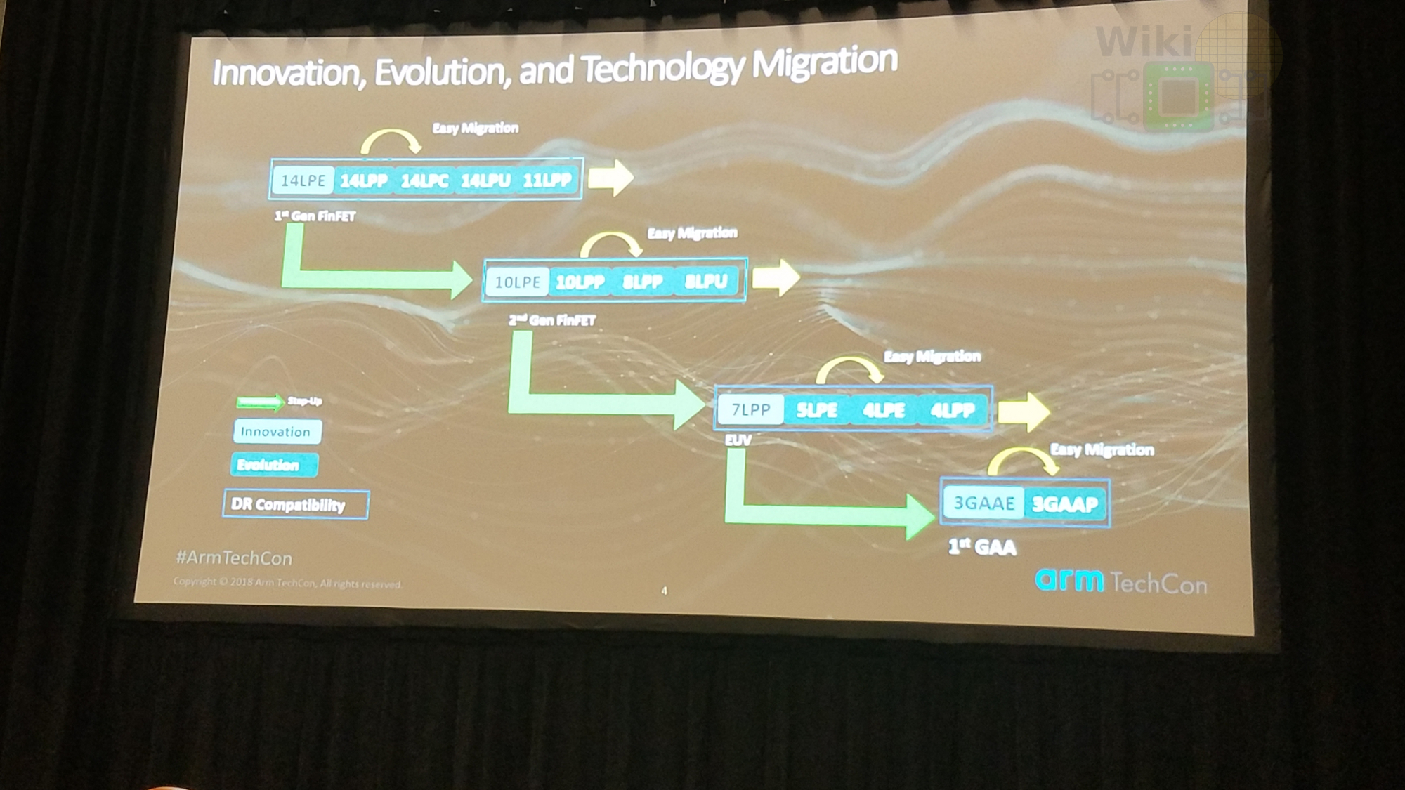
We believe Samsung’s 5-nanometer node is the second-generation 7 nm process Samsung presented at last year’s VLSI.
Related articles:
VLSI 2018: Samsung’s 2nd Gen 7nm, EUV Goes HVM
VLSI 2018: Samsung’s 11nm nodelet, 11LPP
VLSI 2018: Samsung’s 8nm 8LPP, a 10nm extension
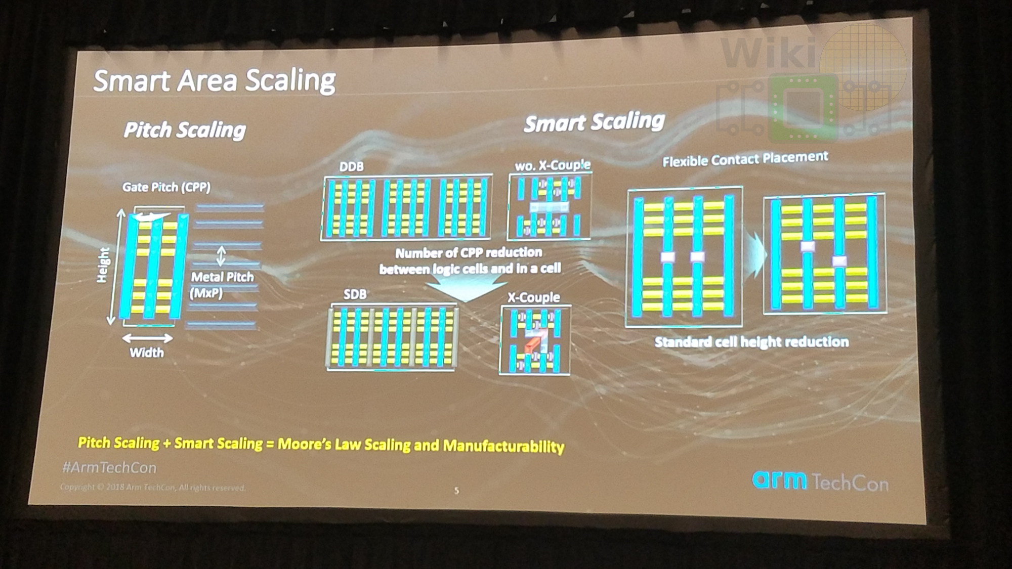
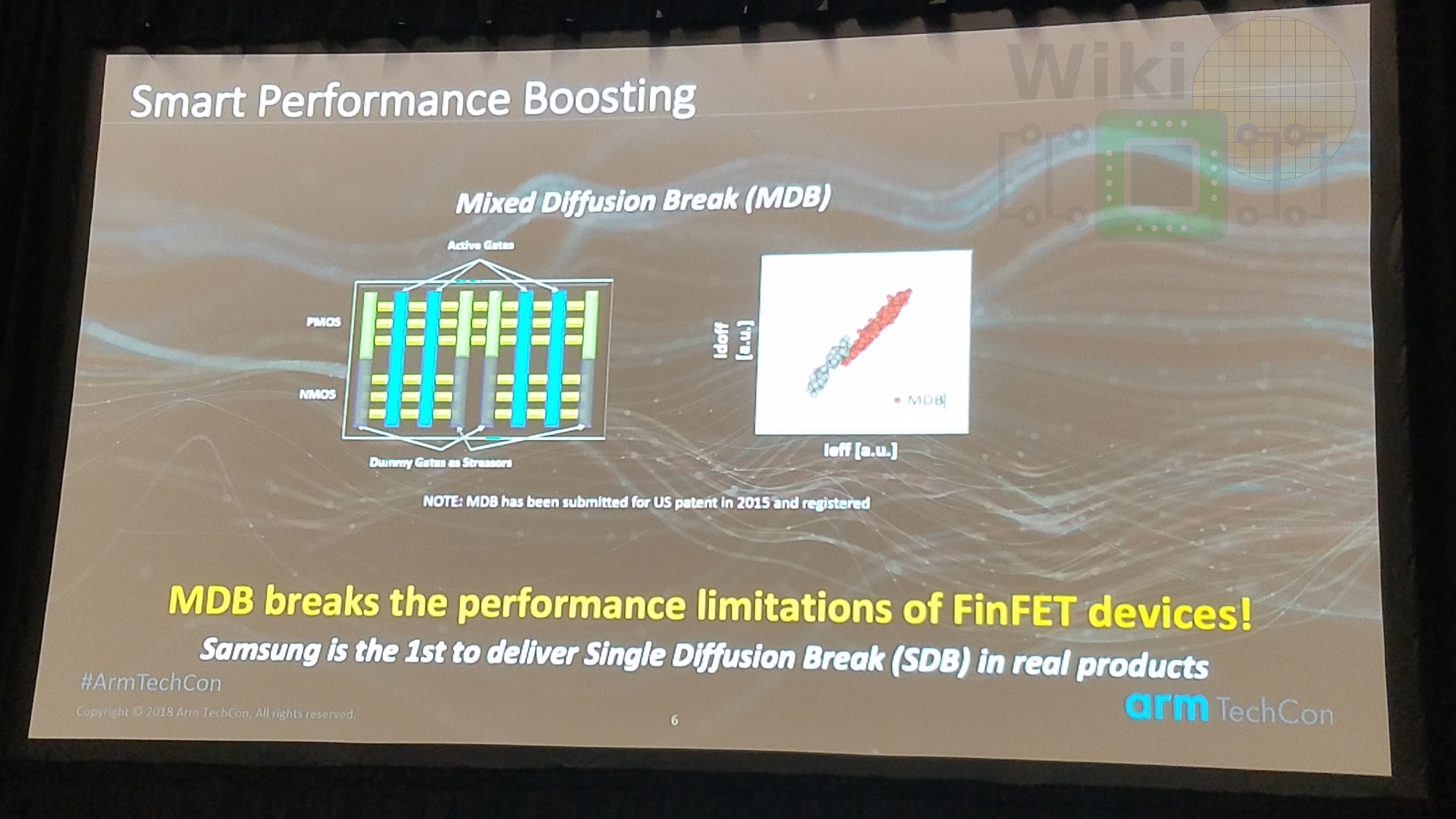
Their 5 nm node re-introduces single diffusion breaks (SDB) and possibly mixed diffusion break (MDB) which they now call Smart Diffusion Break (SDB). This node is largely design-rule compatible with their 7 nm design, putting most of the effort squarely on transistor recharacterization rather than redesign.
| Samsung Technology Comparison | |||||
|---|---|---|---|---|---|
| Technology | 14nm | 10nm | 7nm | 8nm | 5nm |
| Fin | 2nd Gen | 3rd Gen | 4th Gen | 5th Gen | |
| Gate | – | 1st Gen | 2nd Gen | 3rd Gen | |
| S/D Eng | 2nd Gen | 3rd Gen | 4th Gen | 5th Gen | |
| SDB | 1st Gen | 2nd Gen | – | 2nd Gen | 3rd Gen |
| Gate Stack | – | 1st Gen | 2nd Gen | 3rd Gen | |
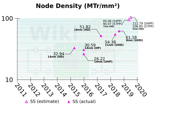
In terms of density, Samsung is reporting up to 25% increase in logic area efficiency through standard cell architectural improvements. We estimate the density at around 112/106 MTr/mm² depending on whether they are using a 54 or 57 nanometers poly pitch (both numbers were thrown around).
6 nm
In addition to the 5-nanometer node, Samsung mentioned a new 6-nanometer node. At one time Samsung had a 6LPE on their roadmap but has long been removed. In fact, no 6 nm was mentioned at the Samsung Foundry Forums late last year either. Not much is known about this node other than they have had a custom tape-out on it. It’s worth noting that TSMC has also announced a new 6-nanometer node today which offers an 18% logic density improvement over their 7 nm node.
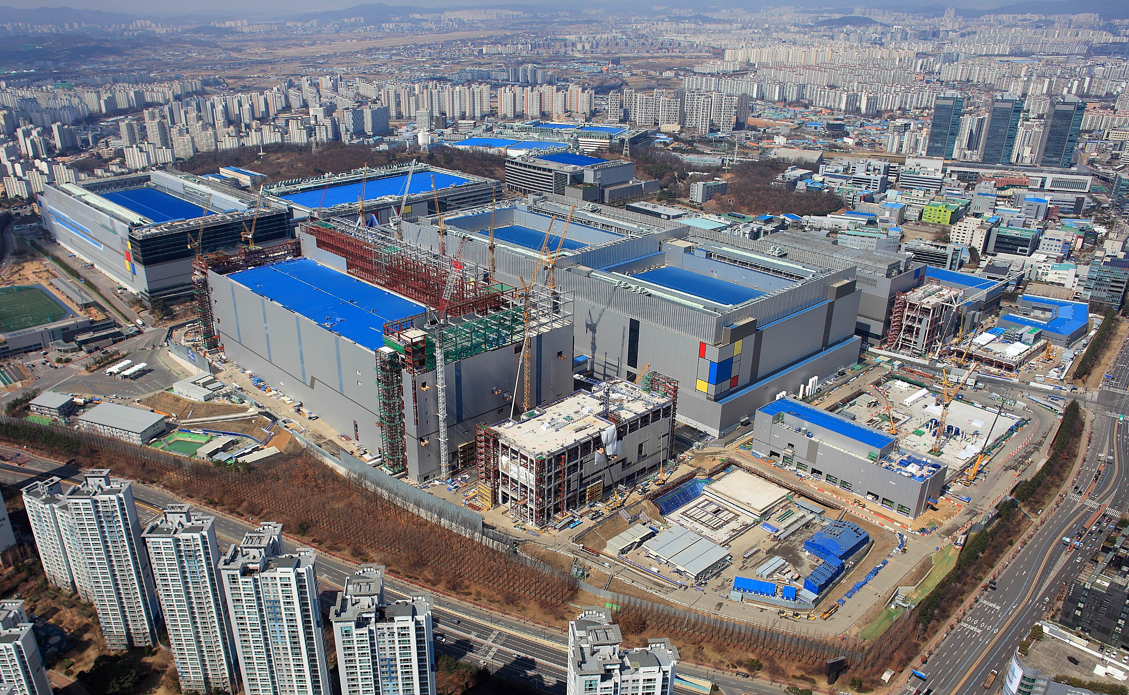
Samsung’s current EUV-based process nodes are being manufactured at their S3 line in Hwaseong, Korea. The company plans on expanding its capacity to a new EUV line in Hwaseong. The construction project is expected to complete by the second half of the year with production ramping up for next year.
–
Spotted an error? Help us fix it! Simply select the problematic text and press Ctrl+Enter to notify us.
–