
TSMC Starts 5-Nanometer Risk Production
Earlier this week TSMC announced that their 5-nanometer process technology has entered risk production. 5 nm PDKs are now available for production design and design components and rules have been delivered to their Open Innovation Platform (OIP), ready for customer designs.
5 nm
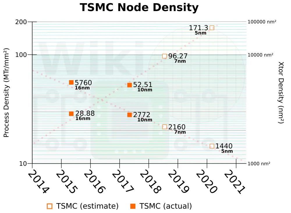
TSMC has not been very forthcoming about their 5 nm (or 7 nm) design rules. TSMC reported a 1.6x compaction ratio compared to their 10 nm node and 3.3x compared to 16 nm. They also reported 35% – 40% speed improvement or >65% power reduction over their 16 nm. We believe they are using a 54 nm gate pitch and a 40 nm metal pitch for their 7 nm node. This yields an estimated logic density of 96.27 MTr/mm².
| Estimated Design Rules For 7 nm | |||
|---|---|---|---|
| 16 nm | 10 nm | 7 nm | |
| CPP | 90 nm | 66 nm | 54 nm |
| MMP | 64 nm | 42 nm | 40 nm |
| Density | 28.88 MTr/mm² | 52.51 MTr/mm² | 96.27 MTr/mm² |
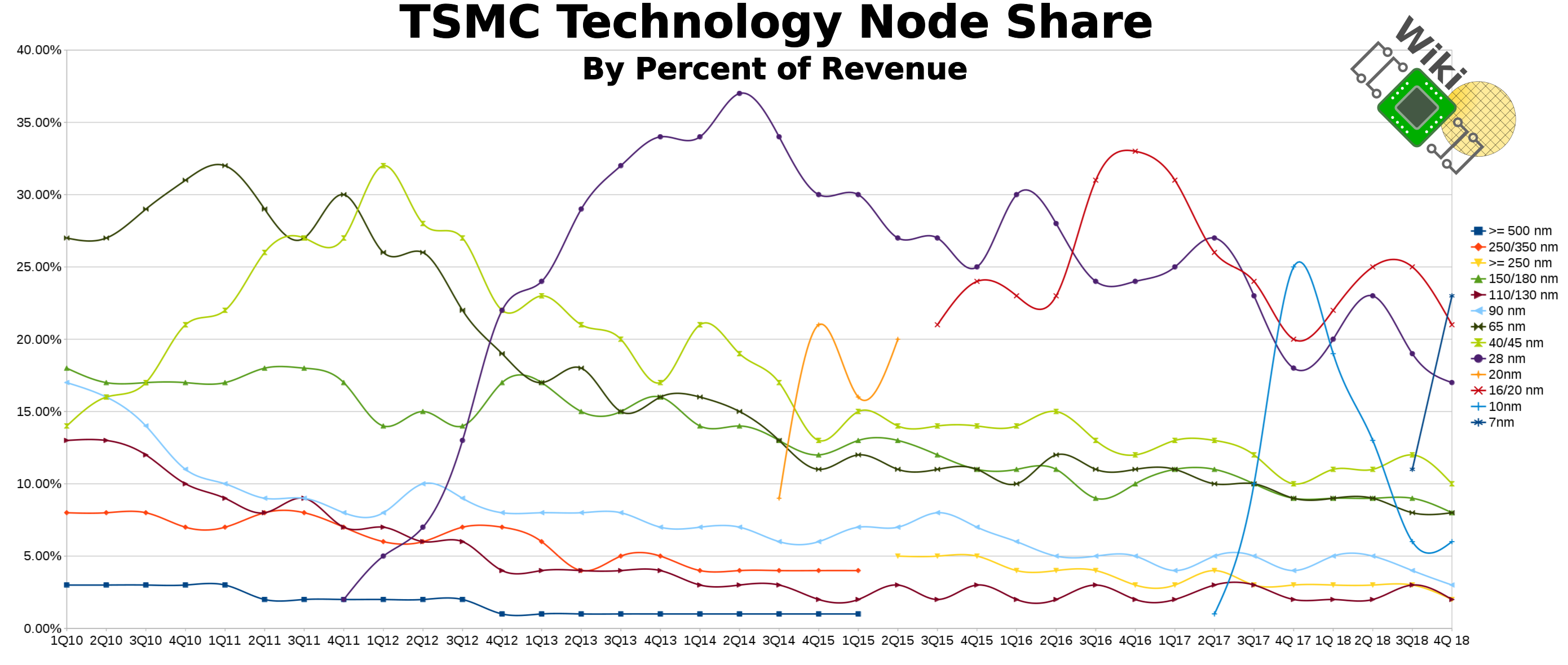
Their 7-nanometer process has been in mass production since last year. As of Q4 2018, the node has accounted for 23% of total revenue.
Their 5 nm node continues to use bulk silicon FinFET transistors. Leveraging their experience from 7+, 5 nm is expected to utilize EUV for more critical layers in order to reduce the multi-patterning complexity. The 5 nm node is expected to deliver a 15% improvement in performance at constant power or a 20% reduction in power at constant performance. TSMC is targeting both low-power mobile and high-performance compute with this node. At the company’s technology symposium last year, it was disclosed that they are targeting a 1.8x compaction ratio compared to their 7 nm DUV node. Based on that, we estimate a gate pitch of 48 nm and a metal pitch of 30 nm for an estimated density of 171.3 MTr/mm².
| Estimated Design Rules For 5 nm | |||
|---|---|---|---|
| 7 nm | 5 nm | ||
| CPP | 54 nm | 48 nm | |
| MMP | 40 nm | 30 nm | |
| Density | 96.27 MTr/mm² | 171.3 MTr/mm² | |
SRAM
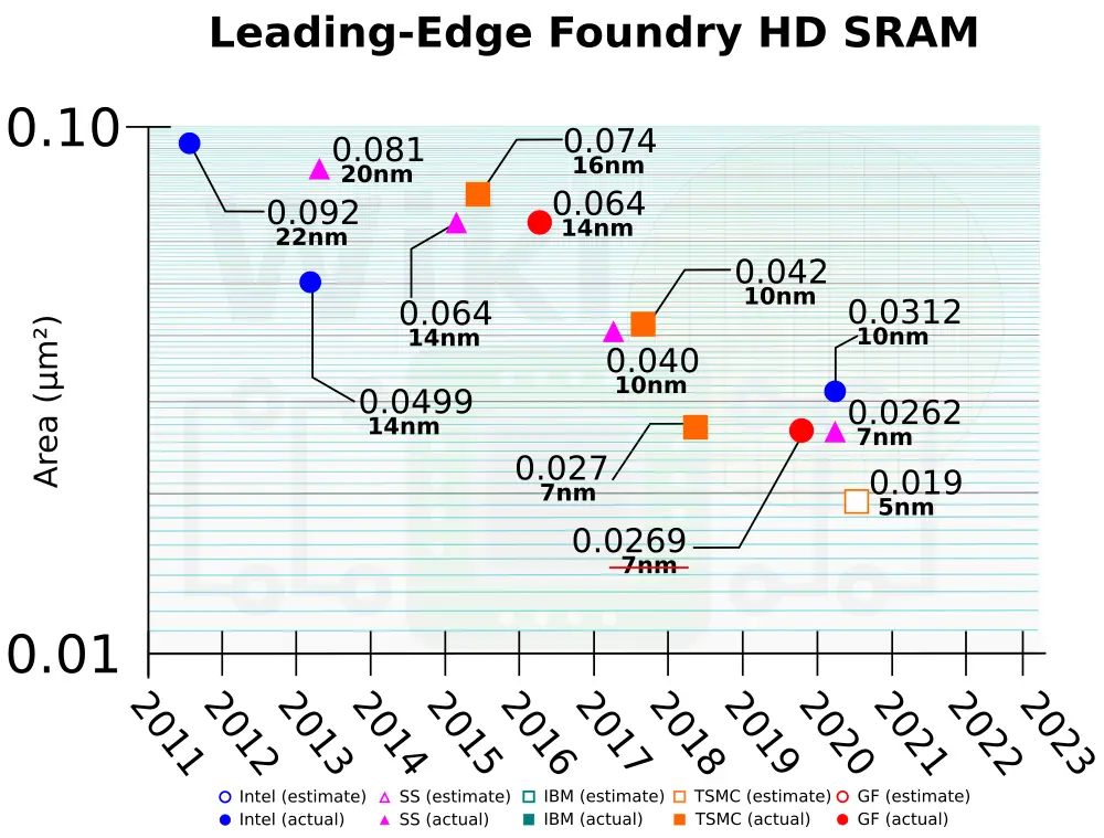
With those estimates, we expect the HD SRAM size for the 5-nanometer node to be around 0.017 µm² (20nm FP) to 0.019 µm² (22 nm FP).
| Estimated 5 nm SRAM | ||||
|---|---|---|---|---|
| 16 nm | 10 nm | 7 nm | 5 nm | |
| SRAM | 0.074 µm² | 0.042 µm² | 0.027 µm² | 0.019 µm² (22 nm FP) 0.017 µm² (20 nm FP) |
At their earnings call in January, TSMC stated they expect 5-nanometer volume production ramp in first half 2020.
–
Spotted an error? Help us fix it! Simply select the problematic text and press Ctrl+Enter to notify us.
–