
A Look at Intel Lakefield: A 3D-Stacked Single-ISA Heterogeneous Penta-Core SoC
Last year Intel announced Lakefield, a realization of decades-worth of research and development. It is an important milestone for the semiconductor industry, not just Intel, due to the technology it pushes into production. It also serves as a guide as to what needs to be improved to fully take advantage of the underlying technologies as they mature.
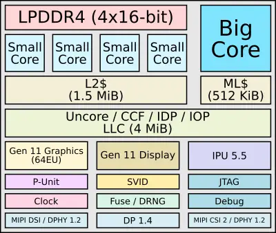
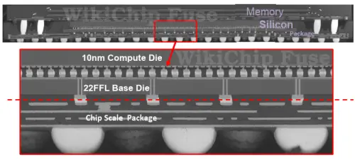
Lakefield is a mobile SoC but differs from Intel’s existing mobile SoCs in terms of board size and power requirements. A number of companies have announced products that will use this chip including the Microsoft Surface Neo and the Samsung Galaxy Book S. Lakefield has unique smartphone-like power requirements such as always-on and always-connected capabilities with around 2 mW of standby power. It also features Intel’s most recent Gen 11 Graphics which is said to bring around 50% performance improvement over the previous generation. Lakefield is interesting for an array of different reasons. First, it’s Intel’s first heterogeneous multi-core architecture. It features an unusual penta-core configuration with a single big core and four small cores along with the company’s new Gen 11 graphics. It utilizes Foveros, the company’s three-dimension IC packaging technology – bonding face-to-face a compute die on top of a base I/O die. Finally, the package incorporates LPDDR4x PoP memory on top. And it’s all within a tiny package measuring just 12 mm by 12 mm by just 1 mm in height. Let’s take a deeper look.
The Base Die
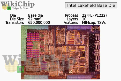
At the bottom of the package, resting on the high-resolution substrate (such as what’s typically used for RF applications) is the base die. Here, Intel threw anything concerning lower-power functionalities like your usual chipset but also includes certain subsystems for always-on and ultra-low power standby functionalities. Some of the interfaces here include USB 3 Type C, Audio, Debug, SDIO, and various other low power I/O components. The base die also includes the PCIe Gen 3 interface.
Measuring just 92 mm², the die is fabricated on the company’s relatively new 22FFL process. It features 10 metal layers, MIM cap, and allows for TSVs from the upper die. The process itself is very different from the older 22 nm node. 22FFL is more of an ultra-low power-optimized derivative of their incredibly successful 14 nm process. It has been optimized for ultra-low leakage and has enhanced analog capabilities. It is also cheap. Being a slightly more relaxed version of 14 nm, the process was restricted to an entirely single-patterning BEOL, thereby significantly reducing the mask count and overall cost.
Further Reading:
IEDM 2017: Intel details 22FFL, a relaxed 14nm process for foundry customers, targets mobile and RF apps – WikiChip Fuse
Compute Die
Resting on top of the base die is the compute die. This is a slightly smaller die – measuring just 82 mm² while integrating just a hair over 4 billion transistors – that is fabricated on Intel’s 2nd-generation 10-nanometer (10nm+) process. As the name implies, this die incorporates all the high-performance components. This includes quad-channel (16b) LPDDR4 memory, the CPU cores, the system agent, the Gen 11 GPU, Gen 11.5 display engine, and the IPU 5.5.
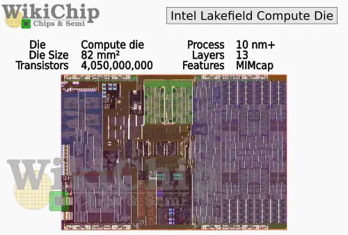
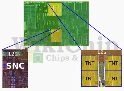
From the die above we can pick up a number of details that were not officially disclosed but are not unexpected. The first is that the SoC itself is very similar to Ice Lake (Intel did say that it’s based on the same chip). It features a system agent, cores, and GPU connected over a bidirectional ring interconnect. Careful scrutiny hints that there are only four ring stops (agents) so presumably there’s one for the GPU, one for the uncore, one for the big core, and just one for the quad-core small core cluster. Intel moved to quad-core clusters with the Goldmont Plus architecture. Doesn’t look like anything too major has changed since.
Beyond the CPUs we do want to point out the amount of silicon dedicated to graphics. Roughly 37% of the entire die is the Gen 11 GPU – not including the IPU 5.5 and Gen 11.5 Display Engine which are the two purplish areas on the left side of the die. In contrast to Ice Lake, some of the silicon area saving came from eliminating the Thunderbolt 3 Type-C (and PCIe Gen 3) interface which has been moved to the base die.
Further Reading:
IEDM 2018: Intel’s 10nm Standard Cell Library and Power Delivery
IEDM 2017 + ISSCC 2018: Intel’s 10nm, switching to cobalt interconnects
Lakefield is unique in its core configuration. This is the first time Intel mixed their big cores with their small cores. Here, there are four Tremont cores along with a single Sunny Cove core for a total of five cores and five threads (note that multithreading is disabled on Sunny cove). Both cores have previously been introduced as a stand-alone product: Sunny Cove was released by Intel in their Ice Lake-based CPUs while Tremont can be found in the recently announced Snow Ridge networking SoCs. Although the Sunny Cove core supports AVX-512, specifically for Lakefield the core is somewhat crippled without any AVX support in order to maintain full single ISA compatibility across all cores for easy workload migration. The behavior of the running workloads is fed back to the OS in order to finely optimize the affinity of workloads to the appropriate cores based on their performance and power behaviors.
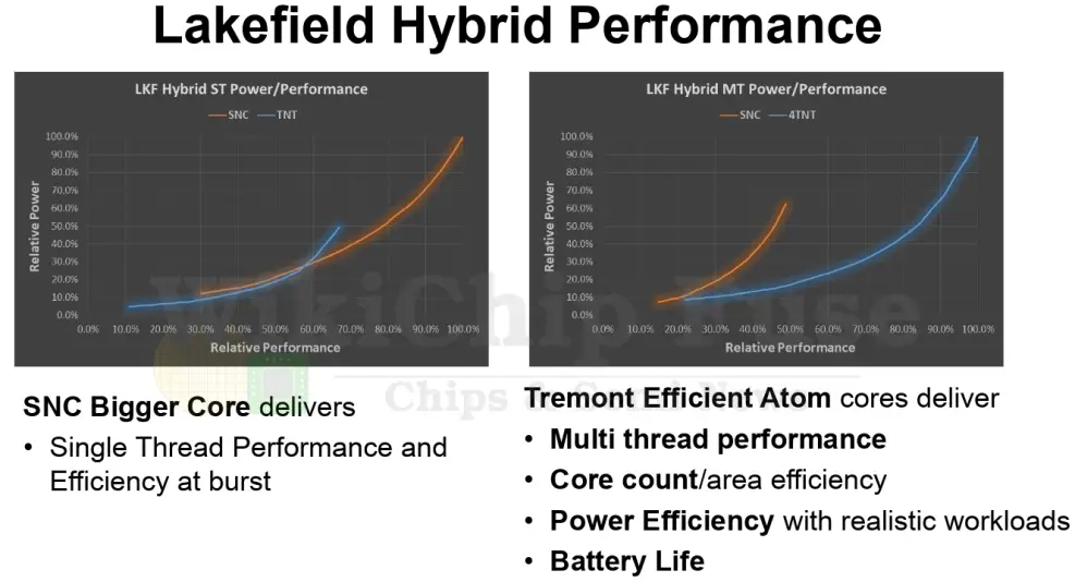
The heterogeneous combination of cores is rather interesting on its own right. Tremont represents a fairly significant uplift in performance and power compared to the last few generations of Atom cores. You are looking at very small cores that can reach the performance of somewhere between Sandy Bridge and Haswell. Intel claims that a single Tremont core can reach up to 70% of the performance of Sunny Cove while beating it in terms of power efficiency. Likewise, in more multi-threaded workloads, a quad-core Tremont cluster is said to achieve as much as twice the performance of a single Sunny Core while offering a considerably better power efficiency curve. By correctly migrating workloads depending on their characteristic the full SoC can achieve better power and performance. Bursty workloads will greatly benefit from the sunny Cove core while more threaded workloads or background workloads can be offloaded to the Atom cores for better efficiency. That is, of course, in theory. In practice, as we’ve seen from the Android ecosystem, good power management is hard and determining which workloads and when to migrate to which cores is no easy task either.
Beyond the performance and efficiency claims, the quad-core Tremont cluster is interesting for another reason – economics. The entire Tremont cluster is almost the same size as a single Sunny Cove core. And just to be clear, we are comparing all four Tremont cores along with their 1.5 MiB of shared L2 to a single Sunny Cove with just its private 512 KiB of L2 cache. By our estimates, the entire Tremont core cluster along with it’s 1.5 MiB of shared L2 cache comes at around 5.14 mm² – with a single TNT core being around 0.88 mm². By comparison, the full Sunny cove core is around 4.49 mm². That’s a substantial size difference. It’s worth noting that even though it’s said to be disabled, the full AVX512 execution units and physical register file still exist in the silicon as can be seen in the die photo.
Stacking
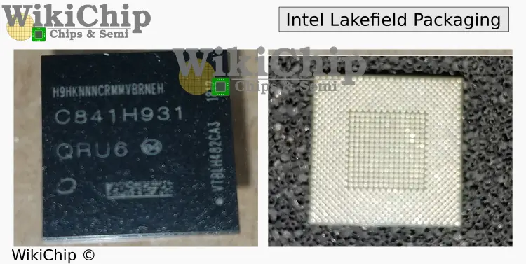
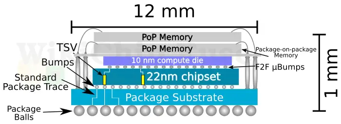
Lakefield is built using Intel’s Foveros 3D packaging technology. The compute die is bonded face-to-face with the base die which sits on the coreless substrate. For Lakefield Intel used 50 um pitch micro-bumps. On top of the Foveros stack, Intel added a couple of LPDDR4 package-on-package memory. Lakefield actually supports two or four high LPDDR4/X DRAM stacks. Memory is incorporated with 350-micron pitch through-mold vias (TMVs). The final chip is a single 12x12x1 mm chip.
Within the Foveros packaging, technology is the 3D inter-die I/O communication interface called the Foveros Die Interface (FDI). FDI includes process-level optimizations and enhancements that were done in order to make sure all the electrical characteristics of the interface are well understood. This includes 3D modeling, optimization, and minimization of ESD between dies, the coupling between layers, and coupling between adjacent bumps. FDI I/O cells sit directly underneath the micro-bumps, eliminating lead-way routing. FDI uses a relatively simple forwarded clocking architecture with the Tx/Rx sitting on the base die supply (for both dies). The interface isn’t very fast, but it’s very wide. The peak data rate is 500 MT/s and bundles 200 lanes with a single forwarded clock. The FDI on Lakefield achieves 0.2 pJ/bit – a roughly 10x reduction from your standard chipset interfaces such as Intel’s OPI (or AMD’s IF). Intel says that this will be further reduced in future products.
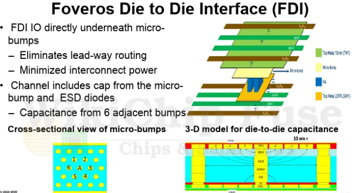
The base die incorporates TSVs for routing signals and power directly to the package. Since the base die is an active interposer, things are a little more challenging. Intel says the TSV rules were designed to allow for high block-level cell utilization of greater than 75%. Additionally, it has been optimized to enable circuit design with SRAM, register files, and I/O in the presence of TSVs. Signal TSVs use an array of 1×1 while power TSVs are built as an array of 2×1, 2×2, 2x3x2 patterns per C4 bump. Intel says the TSV capacitance is 50 fF at frequencies exceeding 1 GHz with a loss of less than < 0.5dB.
Form Factor
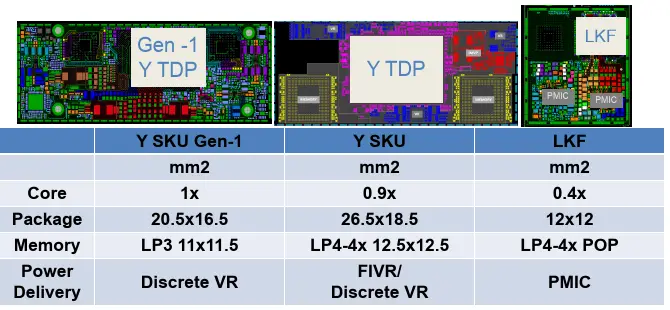
With the DRAM integrated within the package, this chip has a form factor of a smartphone. Intel traditionally has two series of processors called the Y series and U series (such as Ice Lake U and Ice Lake Y). The size difference is quite substantial between Lakefield and the two other mainstream series. It’s worth pointing out that a simple PMIC is used instead of a FIVR or a normal VR that has traditionally been done.
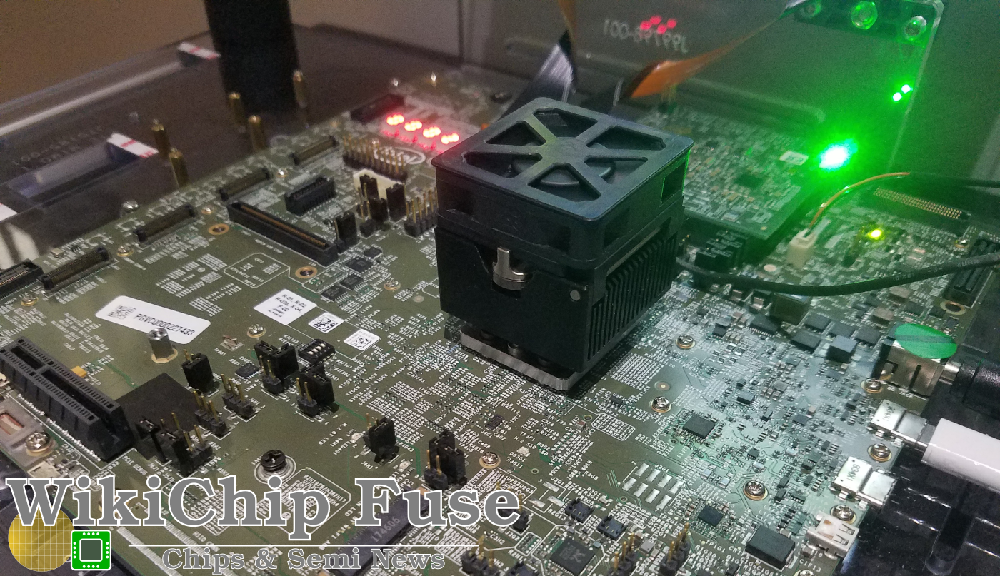
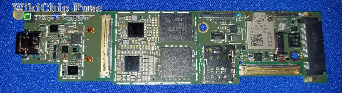
We had an opportunity to check out a board in-person. Although we don’t have a frame of reference, it’s actually very small, about 125 mm by 30 mm or roughly the size of four quarters side by side. Lakefield is the black chip in the center of the board on the bottom.
Room for Improvements
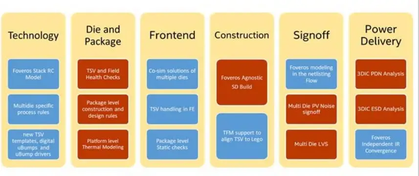
Being the first product to utilize a number of new technologies, Lakefield is also serving as a learning vehicle for all future products. 3D stacking for logic is an emerging technology. To make Lakefield possible, new CAD tools had to be developed along with new system-level co-optimizations. Intel says that both internal and external CAD tools were modified and enhanced to enable 3D IC design citing “new capabilities in construction, place and route, die-to-die timing and modeling, power delivery, ESD, thermals, signal integrity”. Signoff tools were also enhanced for 3D ICs, allowing them to verify full-chip functionality. Nonetheless, CAD tools remain very far behind where the industry needs them to be for better 3D IC development.
Lakefield has a lot of shortcomings. Intel’s long-term goal is to be able to mix-and-match compute chiplets on top of the base die with Foveros. Although there are a growing number of options for chiplet interfaces for 2D and 2.5D interfaces, currently, no standard interface for 3D chiplets exist. Lakefield uses POP memory because of its form factor and cost, however for the memory to reach the compute die it has to go through the copper pillars to the package and through the base die up to the compute die – all of this despite sitting directly on top of the compute die. There is no standard memory interface for 3D ICs such as HBM2 for 2.5D. Intel says that it is working with industry partners on possible solutions.
Next-Gen
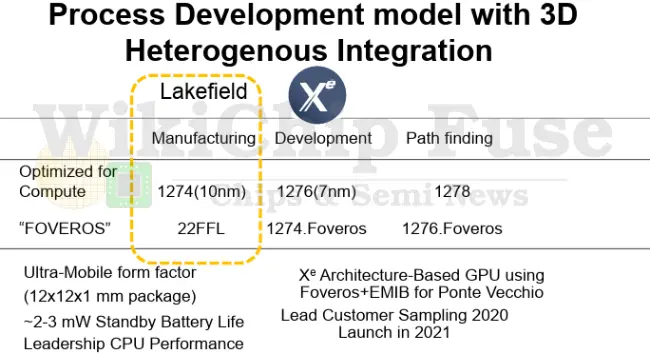
Looking a bit further, Intel has started talking about some of its other packaging technologies. Foveros can and will be used with those other technologies such as EMIB. Intel second-generation Foveros will be manufactured with a compute die on the company’s 7-nanometer process and with a base die on the company’s optimized 10-nanometer process. The lead product and the flagship product to use Foveros and EMIB is the Xe Architecture-based GPU, codenamed Ponte Vecchio. Wilfred Gomes, Intel Fellow and Silicon Engineering Group Director, said that lead customers will be sampling the product in late 2020 and launch in 2021.
–
Spotted an error? Help us fix it! Simply select the problematic text and press Ctrl+Enter to notify us.
–