
VLSI 2018: Next Week’s Samsung and GlobalFoundries Papers
 Next week, the 2018 Symposia on VLSI Technology and Circuits will be held at the Hilton Hawaiian Village in Honolulu and WikiChip will be there to cover the event.
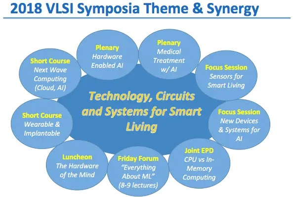
Theme
This year, the conference theme is “Technology, Circuits & Systems for Smart Living”.
Highlights
Though there are many papers being presented, our coverage remains within the scope of logic design. WikiChip has been provided an initial tip sheet which has revealed some interesting information. Below is an early discussion of the paper abstracts and preview.
GlobalFoundries 12nm FinFET
GlobalFoundries will be presenting their 12nm, 2nd generation FinFET, process (12LP). The process is said to provide >10% area reduction including a 7.5T library. 12LP is said to offer around 16 percent power reduction (at fix frequency) or around 15% performance improvement (at a given leakage) over 14LPP with comparable reliability and yield. This process is already used for various products such as AMD’s Zen+ microarchitecture
Samsung 7nm
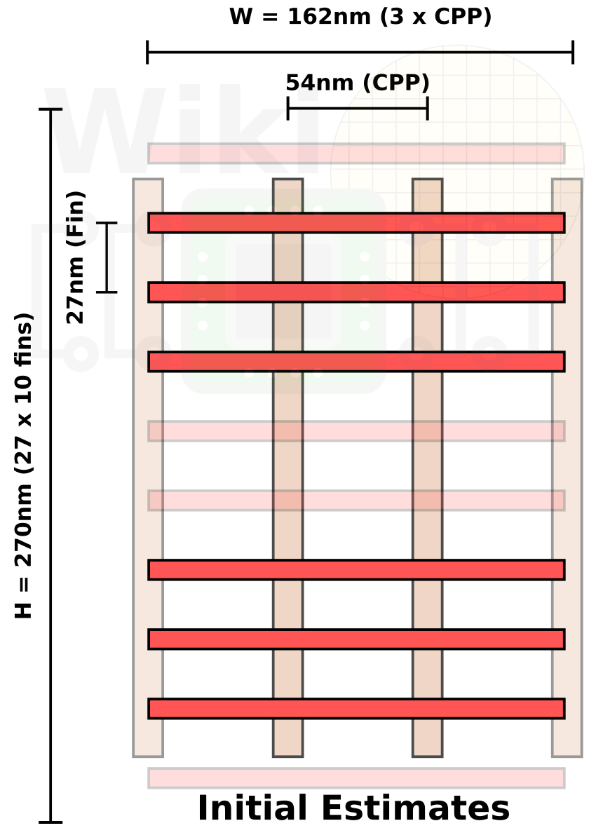
Samsung will be presenting their 7nm platform paper. For their 7nm, Samsung is using single-patterning EUV for the MOL and some BEOL layers. They have revealed that the poly pitch is 54nm and a very dense fin pitch of 27nm. We’ll have to wait for the paper to get the full details but we believe their cell comprises ten diffusion lines. If that’s the case then their cell height appears to be 270nm. Samsung has their own version of Intel’s “hyper-scaling” which include a single dummy gate and “special constructs” which will presumably be discussed in the paper.

If the cell height is correct, then a typical NAND2 cell would look like this.
We will have an updated article at the conclusion of the conference.
Samsung 11nm
Samsung will be presenting their 11nm (11LPP) process which is said to use their 3rd generation 14nm FEOL and their 10nm BEOL process. They have designed a 6.75T library to take advantage of the new process. 11LPP is said to deliver 25% ring oscillator AC frequency improvement or 42% lower power over their first-generation 14nm.
Samsung 8nm
In another paper, Samsung will also be discussing their 8nm (8LPP) node which is said to deliver 15% higher density and 7% lower power compared to 10LPP. The density increase is coming from further cell compaction through a single P fin reduction and a slightly tighter gate pitch. As with their 10nm node, Samsung is also using quad patterning (LELELELE) here.
Snapdragon 845 and 10nm/8nm
Qualcomm and Samsung will be talking about the Snapdragon 845 which was released back in December 2017. The paper will discuss Samsung’s 2nd generation 10nm (10LPP) which helped deliver additional 30-40% performance increase and 10% battery life increase. There will also be some discussion about their 8nm in this presentation.
GlobalFoundries Cu interconnect extension
GlobalFoundries has been working on copper interconnect scalability extension for a while now. This year they are back to talk about their results on laser-induced grain growth within Cu interconnects. They claim a 30% line resistance reduction in Copper interconnects, delivering 15% improvement in RC and IDsat improvement of 2-5%.
Initial Estimates
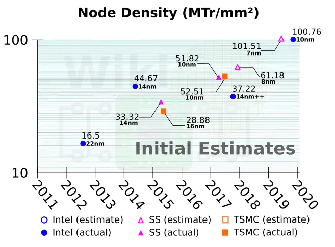
Based on the currently available information, using Intel’s MTr/mm² metric, this is our initial estimates. We will have to wait for the papers to fully confirm the information.
–
Spotted an error? Help us fix it! Simply select the problematic text and press Ctrl+Enter to notify us.
–