
IEDM 2017: Intel details 22FFL, a relaxed 14nm process for foundry customers, targets mobile and RF apps
Ultra-Low Leakage
The performance we talked about earlier is for the standard 22FFL devices which had a fin pitch of 108nm. In addition to those devices, Intel introduced 144nm pitch devices for ultra-low leakage. 22FFL ULL devices have sub-1 picoamp per micron total leakage. Those devices provide up to an additional 75x reduction in leakage.
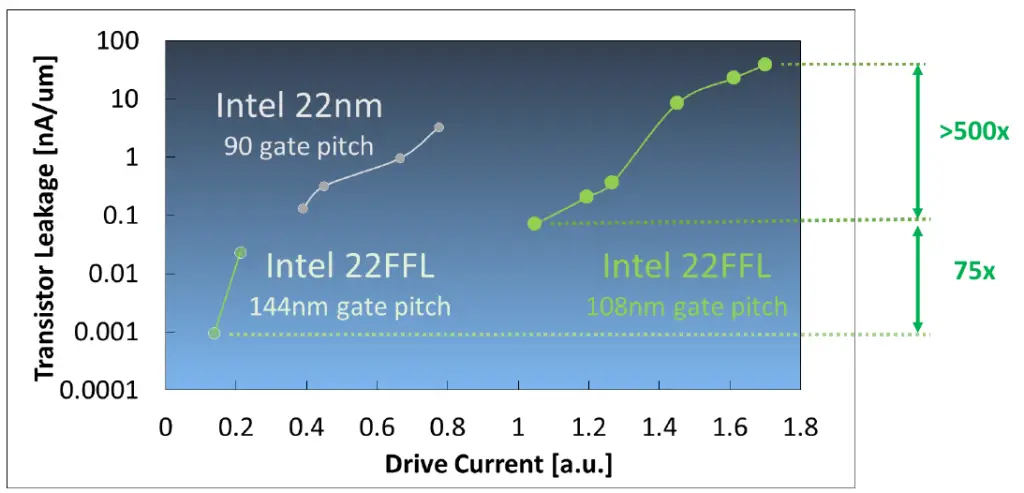
In the graph above, Intel’s original 22nm process (on the upper-left corner) can be used as a reference. The high-performance 22FFL devices start at the very top-right corner. Those six points represent the six devices we mentioned earlier (LP, Nom, HP, LPLVT, LVT, ULVT). There is a range of over 500x between the highest- and lowest- leakage among those devices. The Ultra-low leakage devices can offer an additional 75x reduction in leakage. We believe those are among the lowest, if not the lowest, total leakage logical devices reported with sub 1-picoamp per micron leakage.
Device Summary
We have summarized the three types of logic devices offered by Intel’s 22FFL.
| 22FFL Logic Devices | ||||||||
|---|---|---|---|---|---|---|---|---|
| High Performance | Low Power | Ultra Low Power | ||||||
| Device | ULVT | LVT | LPLVT | HP | Nom | LP | LL | |
| Vdd | 0.7 V | |||||||
| Gate Pitch | 108 nm | 144 nm | ||||||
| Fin Pitch | 45 nm | |||||||
| Tox | Thin | Thick | ||||||
| Performance @ 0.70 V |
nMOS | 1.24 mA/μm | 0.81 mA/μm | 0.10 mA/μm | ||||
| pMOS | 1.22 mA/μm | 0.81 mA/μm | 0.10 mA/μm | |||||
| Ioff | 10 nA/μm | 100 pA/μm | 1 pA/μm | |||||
SRAM
As expected, a number of SRAM bit cells were developed for 22FFL. At their 2017 IEDM presentation Intel reported three cells: high current cell (HCC), high density cell (HDC), and a low leakage cell (HCC-LL). For the HCC SRAM, which is a modified 14nm SRAM, Intel reported a cell area of 0.087 μm² and a low Vmin of 490 mV. The HCC is a slightly bigger cell, reported at 0.107 μm². But if you’re willing to pay for a little bit more area and a bit higher leakage, you get much higher current and even lower Vmin (reported at 440 mV which is actually one of the lowest Vmin reported to date).
The HCC-LL SRAM is based on the ultra-low leakage device with a bit cell leakage of sub-picoamp per bit. Since the Vth is higher for this cell, the Vmin is also higher but has been reported to be around 720 mV. Note that the cell area was not reported.
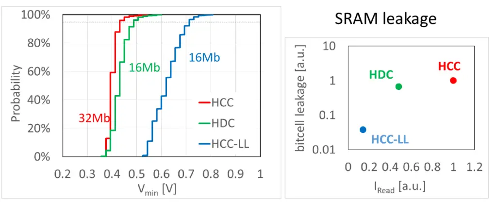
For the graph above Intel’s figure of merit is at the Vmin at the 95 percentile. Those values were obtained based on 9000 dies of 16 Mib and 32 Mib 6T SRAM arrays at worst case after stress testing.
| 22FFL SRAM | |||
|---|---|---|---|
| Type | HCC | HDC | HCC-LL |
| Area | 0.107 μm² | 0.087 μm² | N/R |
| Vmin | 440 mV | 490 mV | 720 mV |
N/R – Not reported
Analog Devices
The good logic characteristics also transfer to analog transistors. Intel presented three analog devices. Since the Rout is proportional to the channel length, those three devices have channel lengths of 144nm, 216nm, and 270nm.
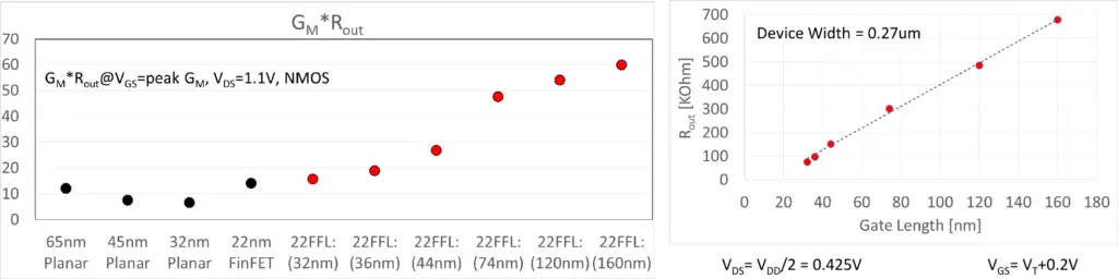
For their longest channel length devices with 6 fins Intel reported an Rout of 0.68 MΩ. In the graph above, the black points are Intel’s previous technologies. They use GM * Rout as a way of comparing the performance of their transistors. The first few red points are actually the logic 22FFL devices which also have a better GM*Rout then their old technologies but for the analog devices with much bigger channel length the improvement is pretty substantial.
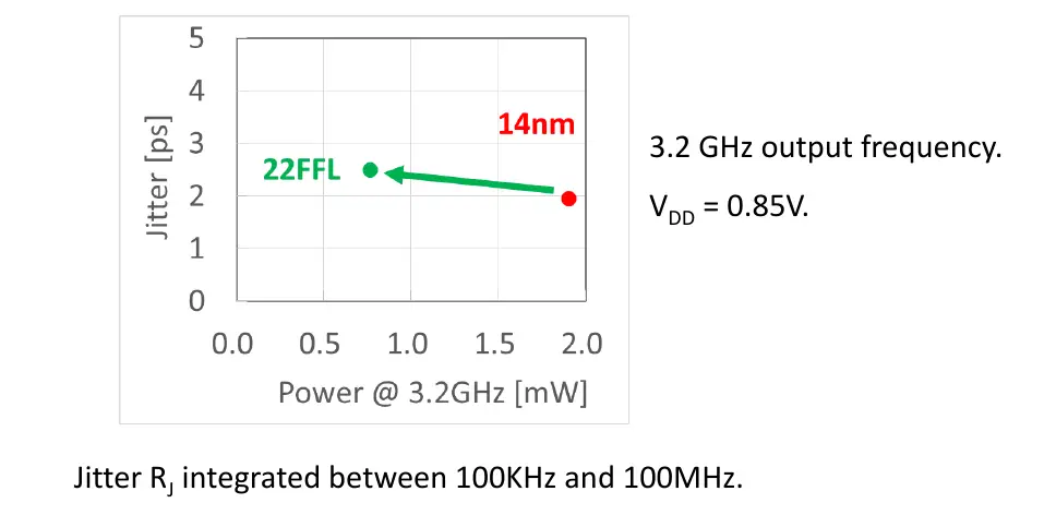
At IEDM they presented a PLL which was designed with those analog devices. At 3.2 GHz output frequency and 0.85 volt Intel reported 0.77 mW of power. An almost identical device was actually presented a few years ago at IEDM for their 14nm process. Compared to the PLL device implemented on their 14nm, the 22FFL PLL gets much lower power for roughly the same jitter.
–
Spotted an error? Help us fix it! Simply select the problematic text and press Ctrl+Enter to notify us.
–