
IEDM 2017: Intel details 22FFL, a relaxed 14nm process for foundry customers, targets mobile and RF apps
I/O Transistors
22FFL offers I/O transistors which operate at the higher voltage of 1.8 volts. Those transistors are very similar to the logic devices. They have a straight fin with an identical pitch of 45 nm consisting of a high-κ metal gate with strained channel process. Those devices use a gate length of 160nm. Below is the cross section of the fin shown in the left image and a cross section of the gate on the right.
Three thick gate devices were developed to support 1.8 V, 1.5 V, and 1.2 V operations. Those transistors have gate length of 90 nm, 120 nm, and 160 nm respectively (for comparison LL logic Lg = 74 nm). For those devices Intel reported very good drive currents which are considerably higher than what they had in their previous 22m technology. For nMOS they reported around 1.11 mA/um and for pMOS it’s around 1.02 mA/um for the highest voltage cells.
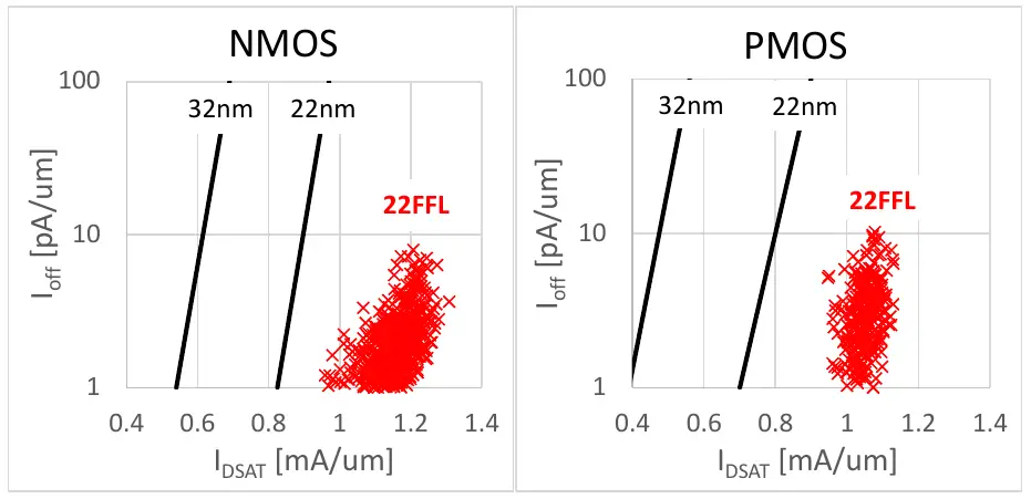
Overall, drive current for 22FFL high voltage transistors are roughly 33% for nMOS and 35% for pMOS over their original 22nm process.
Device Summary (Analog and I/O)
We have summarized the six types of analog and high voltage devices offered by Intel’s 22FFL.
| 22FFL Analog and I/O Devices | ||||||||
|---|---|---|---|---|---|---|---|---|
| Analog Transistors | High Voltage Transistors | |||||||
| Device | AL | AL | AL | TGLV | TGMV | TGHV | ||
| Vdd | 0.7 V | 1.2 | 1.5 | 1.8 | ||||
| Gate Pitch | 144 nm | 216 nm | 270 nm | 216 nm | 216 nm | 270 nm | ||
| Fin Pitch | 45 nm | |||||||
| Tox | Thin | Thick | ||||||
| Perf Unit | GM*Rout | IDSAT (NMOS/PMOS) | ||||||
| Performance | 47 | 54 | 60 | 0.77/0.61 mA/μm | 1.01/0.87 mA/μm | 1.11/1.02 mA/μm | ||
RF Devices
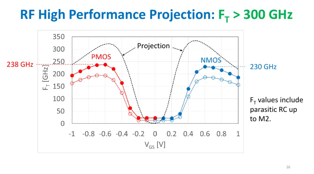
One of the more important aspects of 22FFL is its RF characteristics which Intel clearly spent a lot time enhancing. The graph below shows FT (in GHz) has a function of gate-source voltage. At IEDM they presented an RF standard device on 22FFL which is shown in the open circles. It shows a good balance between nMOS and pMOS with around 180 GHz for nMOS and around 190 GHz for pMOS. Based on that standard device, they also presented an improved high-density device which is shown in the shaded circles. This device reached 238 GHz for pMOS and 230 GHz for nMOS. Ben explained that they plan on improving this device further where they expect to deliver a high-performance device which can go above 300 GHz in their next round of improvements. The projected high-performance RF device is shown in black on the graph. It’s worth noting that all FT values do include parasitic RC up to the Metal 2 layer.
In order to compare their 22FFL RF devices with their older technologies, they presented a plot of FT over GM/ID. GM/ID is a figure of merit that Intel’s RF designers use which should be around 10 or higher. Values less than 10 mean the device is wasting too much power resulting in a very inefficient design. In other words, it’s not enough to just compare the maximum FT of the device, we must consider how much of that is usable in practice.
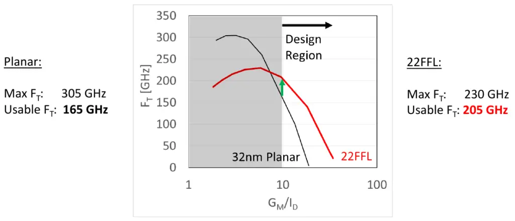
The black line on the graph is a 32nm planar RF device featuring a reported device with an FT of 305 GHz. However when plotted against GM/ID it’s pretty clear that much of it isn’t very good for efficient designs. In fact the highest usable FT, or the highest FT that falls within a GM/ID of 10 or higher, is actually around 165 GHz. Therefore, despite being called a 305 GHz device, the actual usable FT is only around half of that value at around 165 GHz. On the other hand, for the 22FFL RF device, despite having a max FT of 230 GHz, much of the curve falls within a GM/ID of 10 or higher making the highest usable FT somewhere around 205 GHz.
A similar explanation was given for the FMAX of their RF device. The starting standard RF device delivered an FMAX of 242 GHz for pMOS and 284 GHz for nMOS. That’s shown on the graph below in open circles. They improved the process further which resulted in an FMAX of 290 GHz for pMOS and 357 GHz for nMOS.
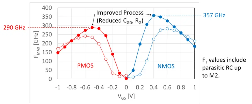
Much of that improvement came from reduced gate capacitance and reduced gate resistance.
As with the FT, Intel plotted the FMAX over GM/ID in order to show the acceptable design region (10 or greater).
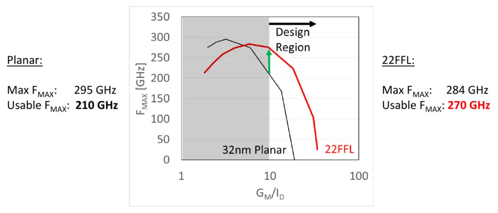
On the 32nm planar process you can make an RF device with a max FMAX of around 295 GHz, however the usable FMAX for that device is only around 210 GHz when within the acceptable design region. When compared to the 22FFL RF device which has a max FMAX of around 284 GHz, we can see that almost the entire peak of the curve falls within the design region with a usable FMAX of 270 GHz.
–
Spotted an error? Help us fix it! Simply select the problematic text and press Ctrl+Enter to notify us.
–