
IEDM 2017: Intel details 22FFL, a relaxed 14nm process for foundry customers, targets mobile and RF apps
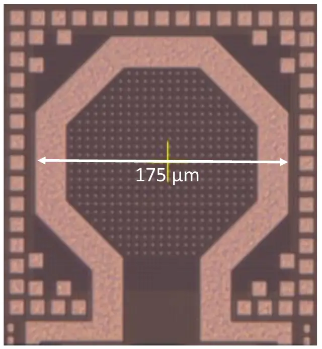
Metal 8, Good for Inductors
Earlier, when discussing the metallization stack, we mentioned that the upper-most layer (M8) had a second function. It was designed to allow for the design of high-Q inductors. To demonstrate this, inductors of different sizes were tested in order to determine the size for the best quality factor. Below is the inductor layout cell which has a very simple design and was fabricated on the Metal 8 layer.
The graph below on the left shows the inductance for the various lengths.
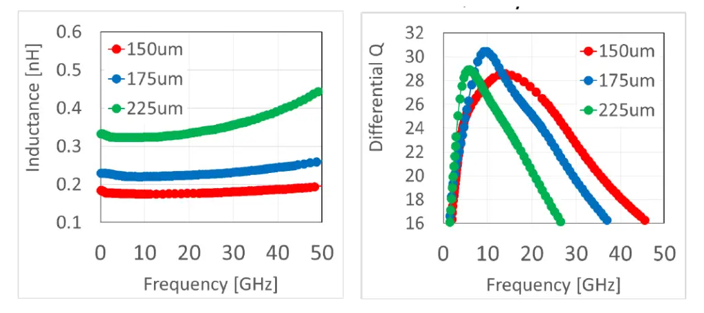
As expected, by increasing the coils diameter or making the core longer, we increase inductance. However the when you compare those sizes against the graph of the quality factor, it’s clear that the 175-micron inductor (in blue) has the highest differential quality factor of over 30 Q.
22FFL
Intel’s 22FFL IEDM presentation was much more detailed but we think we touched on most of the important points.
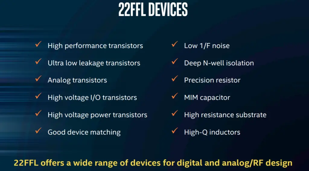
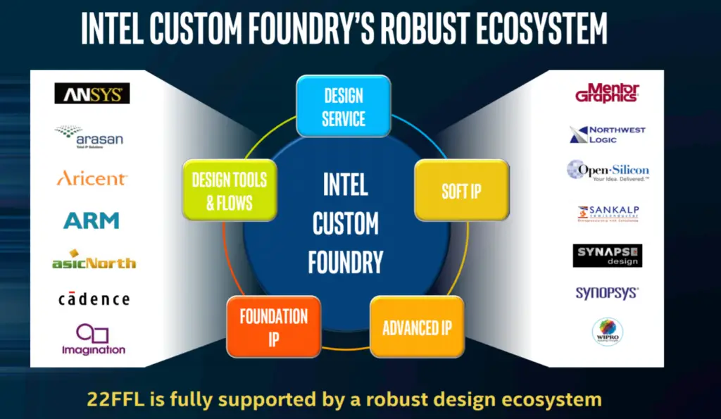
Unlike their own advanced process which has draconian design rules, 22FFL is specifically designed for their foundry customers with low-cost and ease of use first and foremost. They offer high-performance transistors which are a relaxed version of their 14nm process which offers 57% nMOS and 87% pMOS drive gain over their own 22nm. They also also offer ulra-low leakage devices with sub 1-picoamp per micron leakage. They demonstrated SRAM of various designs including a record low SRAM Vmin cell. Additionally, the technology offers high-voltage (1.8V) transistors for I/O with >1mA/um and RF devices with FT / MAX of over 230 GHz and 290 GHz.
A Change of Plan? Going 6T
Just before publishing this article we went over our notes from Intel’s Technology and Manufacturing Day which was held back in March. What caught our eye was the following slide:
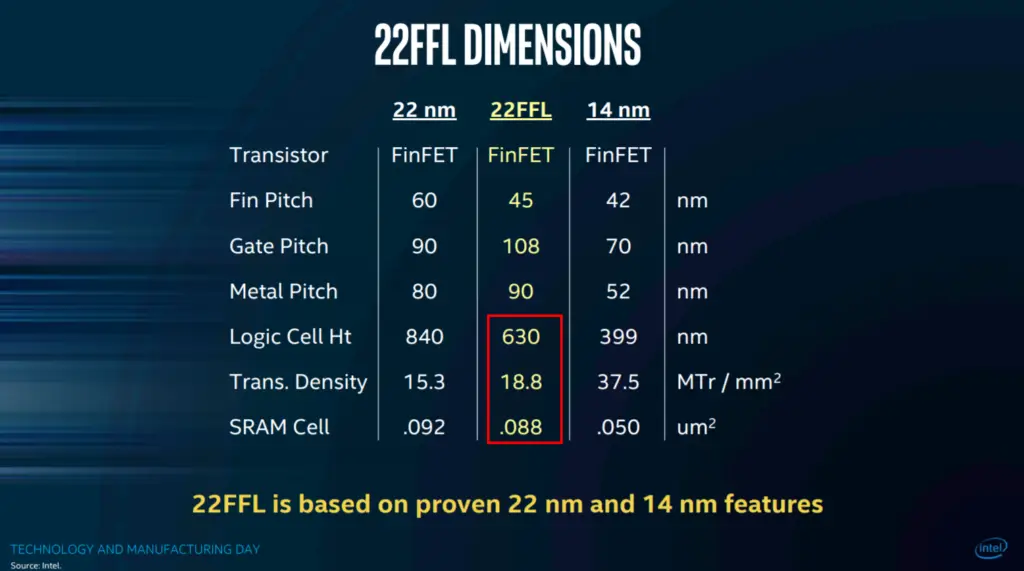
We have highlighted in red the three interesting dimensions – a 7-track logic cell with a height of 630nm, an SRAM of 0.88 μm² and a density of 18.8 MTr/mm². What they presented at IEDM was 6-track logic cells with a height of 540nm, and SRAM of 0.87 μm² which implies a density of well over 20 MTr/mm². That’s a fairly large change from the initial March values to what was presented at IEDM.
Conclusion
Over the last few years, Intel has been trying to grow its custom foundry business. In the past year we have seen a much more aggressive push with the announcement of their custom foundry 22FFL and 10nm HPM/GP technologies. Intel has stated that their 22FFL FinFET technology is cost competitive with other pure-play planar 22nm and 28nm technologies. Overall 22FFL seems to be an excellent process for low-cost, high-performance mobile and RF applications. PDK 0.5 was available as early as April of this year with PDK 1.0 introduced not too long ago. We expect 22FFL to be production-ready in the very near future. Customers will be doing their own analysis and run their own simulations and benchmarks and make their own educated conclusions. Only time will tell if they succeed in attracting new foundry customer.
–
Spotted an error? Help us fix it! Simply select the problematic text and press Ctrl+Enter to notify us.
–