
Intel Looks to Advanced 3D Packaging For More-than-Moore to Supplement 10- and 7-Nanometer Nodes
Complementary Technologies
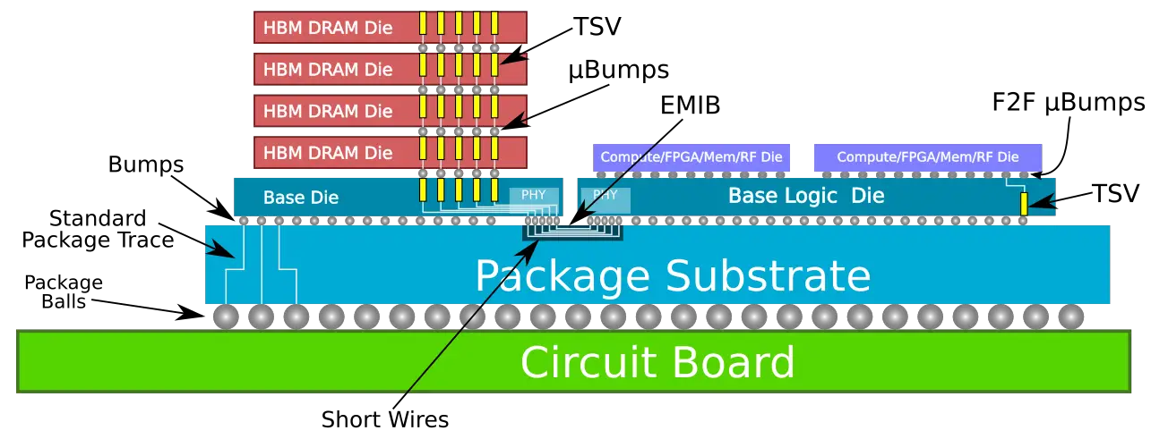
It’s important to note that Foveros was not designed to replace EMIB, it compliments it. The two technologies solve slightly different problems. In fact, the two technologies may even be combined to form even more complex products. In a discussion with Jim Keller, he mentioned that Intel is working on products that use both technologies together. The two technologies are two additional tools for Intel to use where it makes sense. That being said, the standard package is here to stay as well. There will always be cases where the best solution is to use a standard package.

It’s possible we might also see a combination of existing 2.5D and 3D with something like HBM and Foveros stacked dies.
Intel says they are experimenting with all kind of interesting combinations to see what works and what doesn’t.
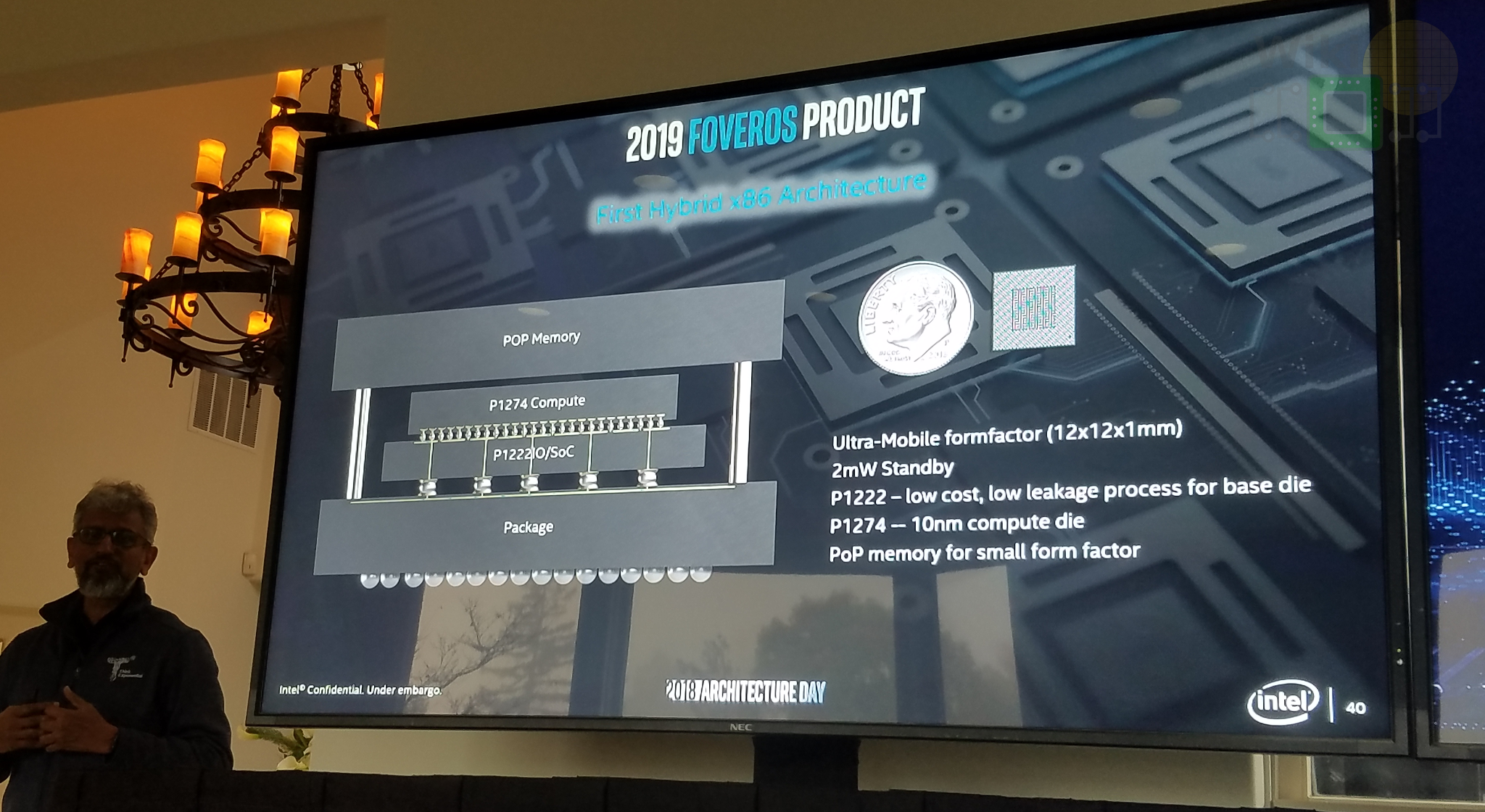
2019 Foveros Product
In addition Foveros, Intel announced the first product to use the technology – a hybrid x86 ultra-low power mobile processor. The chip will be available next year. Intel says the product started out as a request by a customer of theirs who wanted a chip in a package smaller than a typical smartphone chip with x86 cores and an ultra-low leakage of just 2 milliwatt standby power (16 days). The chip will be available as a general OEM product starting next year.
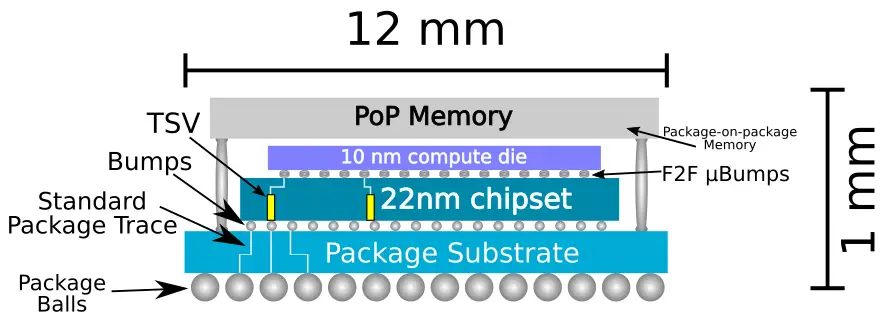
The chip is tiny – 12 mm by 12 mm with a z-height of just one millimeter.
The packaging is a bit more involved. There is a 10 nm compute die on top of an ultra-low leakage chipset base die. Intel also added a package-on-package (PoP) memory to keep everything in a tiny small factor.
Beyond the packaging technology, the chip is very special from an architectural standpoint. This is the first hybrid x86 chip. It features one large big core and four small cores. Presumably, this means the big core is Sunny Cove which will be found in future Core products and the four small cores are Tremont which will be found in future Atom products. The big core comes with 512 KiB of mid-level cache while all four small cores come with another 1.5 MiB of L2 cache. Note that the slide specifically said “MLC” for the big core and “L2” for the small cores so there is some kind of distinction between the two. It’s possible that the big core comes with an L2 cache internally as well. Unfortunately, our photo of the slide was rather blurry. For your convenience, we recreated the block diagram below.
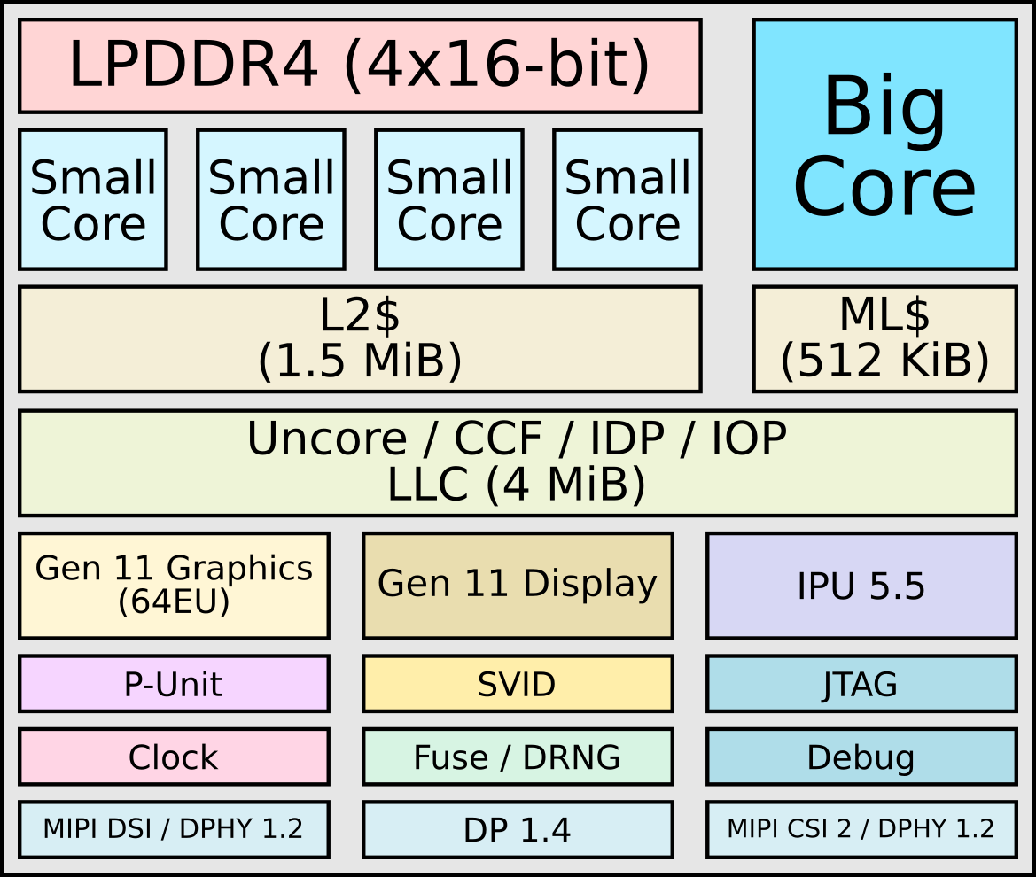
Beyond the mid-level cache, there is 4 MiB of additional last level cache presumably shared by everything. The chip will come with quad-channel LPDDR4 support (4×16-bit) and feature Intel’s Gen 11 graphics with a whopping 64 EUs. That’s 2.5x the amount found in today’s Coffee Lake chips with GT2 Gen 9.5 graphics. There is a new Gen 11.5 display controller, a new image processing unit, and various other I/O.
Intel had an early version of the product on display at the event. It sits under that tiny heatsink and fan. Note that the retail products will be fanless designs with sub-7 W TDP.

They had a simple demonstration of the chip. It was running on just the small cores. There was also a video playing the entire time. The big core was in a parked state (C6). Resizing the video or pressing the windows key will unpark the core and do some useful work after which the core goes immediately back to being parked. The entire process is pretty quick, in line with Speed Shift-level of responsiveness you can find on Coffee Lake.

This is the first disclosure of the hybrid chip. Intel says they will give out more information as they get closer to launch time.
Future FPGA Products
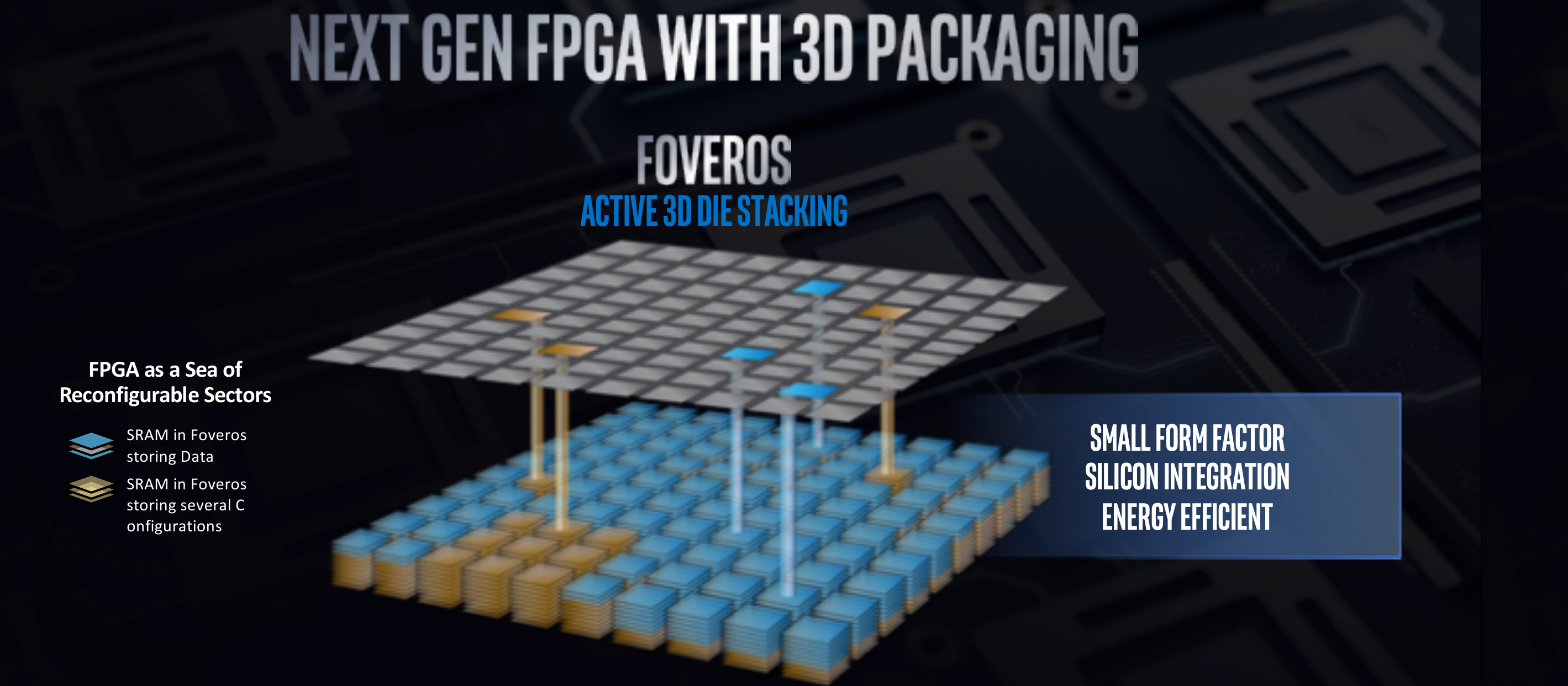
Looking a little further ahead, Intel also has plans to use Foveros for FPGAs. Intel’s next-generation FPGAs will make heavy use of chip stacking. The company expects Foveros to enable 1 or even 2 order of magnitudes increase in terms of performance, energy efficiency, or density compaction. The improvement comes from an entirely different way of configuring the FPGAs. To feed the high-end FPGAs today, the industry uses high-bandwidth memory which is connected through wires across all the configurable blocks. “With Foveros and 3D stacking, all of a sudden, you now have a sea of reconfigurable cores,” says Ravi Kuppuswamy, VP and GM of Intel’s Programmable Solutions Engineering Group. The major simplification comes from their ability to convert the traditionally long wires to short vertical ones.
–
Spotted an error? Help us fix it! Simply select the problematic text and press Ctrl+Enter to notify us.
–