
Nvidia Inference Research Chip Scales to Dozens of Chiplets
Loading Data (PEs)
The actual tiling is software programmable with the only fixed constraint is that there are only eight input and output channels in the processing elements (detailed in the next section). Data arrives at the global buffer of each chiplet. Within the individual dies, the distribution of weights and inputs follow an identical scheme to that of the package-level distribution. Inputs are propagated across the processing elements while the cross-PE output accumulation cascade down.
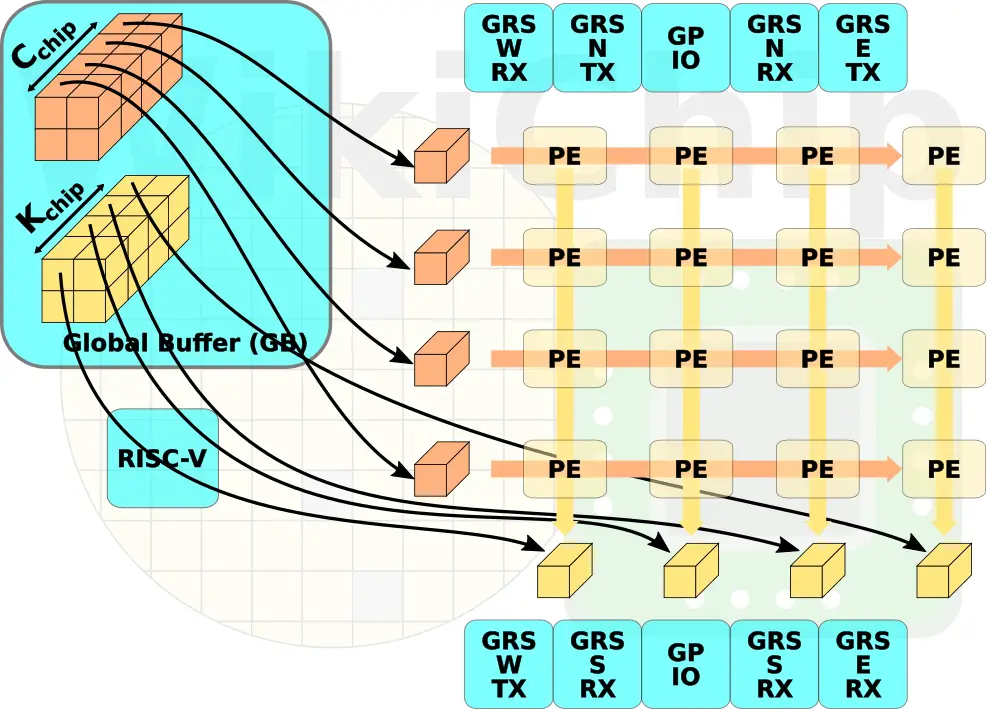
Processing Element
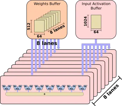
The processing elements are the workhorse execution units of the chip. The PEs operate autonomously without any global synchronization logic apart from the beginning and end of operations. Operations start after coming out of reset. At this point, weights come in and are densely stored in the local 32 KiB weights buffer. Likewise, the input activations are fed into the local 8 KiB activation buffer. When all the data is available, MAC operations can begin. There are eight lanes and each one corresponds to an output channel. Different weights are read into each of the lanes with input being shared across all the lanes after having read once.
Each lane is an 8-wide vector MAC element operating on eight input channels simultaneously. With eight lanes, you are looking at a peak compute of 64 MACs per cycle. The PE reads from the weight buffer every PxQ (the width and height of the result of a convolution) cycles while reading from the input buffer every cycle.
Keep in mind that the workload is split up among all the PEs. Since each PE is working on a subset of the channels, the final values have to be shipped out across PEs in order to aggregate the outputs. Finally, the output activation is computed.
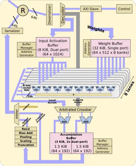
Each PE is capable of 64 8-bit multiply-accumulate per cycle. With 16 of those PEs per chip, there is a total of 1024 MACs executions per cycle.
Performance
Several fairly outdated networks were used for testing. On AlexNet they reported a measured latency of 32,369 cycles which equates to 75% utilization. Strong scaling was demonstrated with ResNet-50. It also showed that a sizable portion of the time is spent with the multi-chip RISC-V synchronization operation. All in all, a single chip can operate from 161 MHz to 2 GHz consuming 30 mW to 4 W with a performance ranging from 320 MOPS to 4 TOPS. For the largest configuration of 36 chips, up to 128 TOPS can be achieved operating at 1.8 GHz and consuming around 110 W.
| Research Chip 2018 | |||
|---|---|---|---|
| 1 Chip | 4 Chips | 36 Chips | |
| Frequency | 161 MHz – 2001 MHz | 515 MHz – 1998 MHz | 484 MHz – 1797 MHz |
| Core Power | 30 mW – 4.16 W | 630 mW – 16.42 W | 5.31 W – 106.09 W |
| GRS Power | N/A | 215 mW – 220 mW | 3.84 W – 4.09 W |
| MACs per cycle | 64 x 16 1,024 |
64 x 16 x 4 4,096 |
64 x 16 x 36 36,864 |
| Performance | 320 MOPS – 4.01 TOPS | 3.93 – 15.7 TOPS | 32.5 – 127.8 TOPS |

Further Analysis
The first thing that should be noticed is that the whole aspect of a memory controller is missing. Currently, an FPGA with a low-bandwidth memory system is employed. Models are operated layer by layer. The current design assumes that everything fits on-chip as well. With the FPGA doing some heavy lifting, it would be interesting to see how a distributed memory controller on-die would have to be implemented to support this functionality entirely on-chip in a scalable way. This also has to take into consideration of the original scaling requirements. With scaling from milliwatts to 100s of watts of power budget, one can expect similar scaling for the memory budget and capability.
The die itself is small. The chip-to-chip interconnects make up a large part of the die and is far from being fully utilized. The small die used for this research was part of their constraint which is understandable. By our measurement, the transceivers are taking up roughly thirty percent more silicon than the processing elements. Ideally, a beefier die with a much larger mesh of processing elements is more desirable. The interconnect will be more than capable of supporting this and each chiplet will end up being more balanced.
There is also the aspect of further scaling. The GRS Nvidia developed is designed to scale to not only other dies in the same package but across multiple packages. It does not look like Nvidia experimented with scaling out into a more massive system, but it would certainly be interesting to see how well things scale with 144 chiplets and half a peta-ops (POPS) of compute.
Foreshadowing
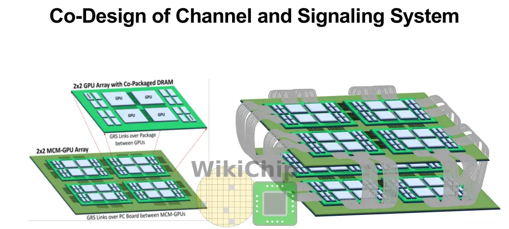
This chip allows Nvidia to survey the impact of various technologies including their ground-referenced signaling link they have been working on for over half a decade. At last year’s VLSI Symposium, Bill Dally gave a keynote where he suggested that similar signaling technology will enable Nvidia to scale as producing smaller dies becomes advantageous as leading-edge nodes continue to rise in cost. One idea he outlined is a 2×2 GPU array with co-packaged DRAM. This board would then be integrated on a larger board with 2×2 such boards for a total of 16 GPUs. He further suggested that those boards could then be scaled in a mesh torus topology.
–
Spotted an error? Help us fix it! Simply select the problematic text and press Ctrl+Enter to notify us.
–