
Intel Cascade Lake Brings Hardware Mitigations, AI Acceleration, SCM Support
DL Boost
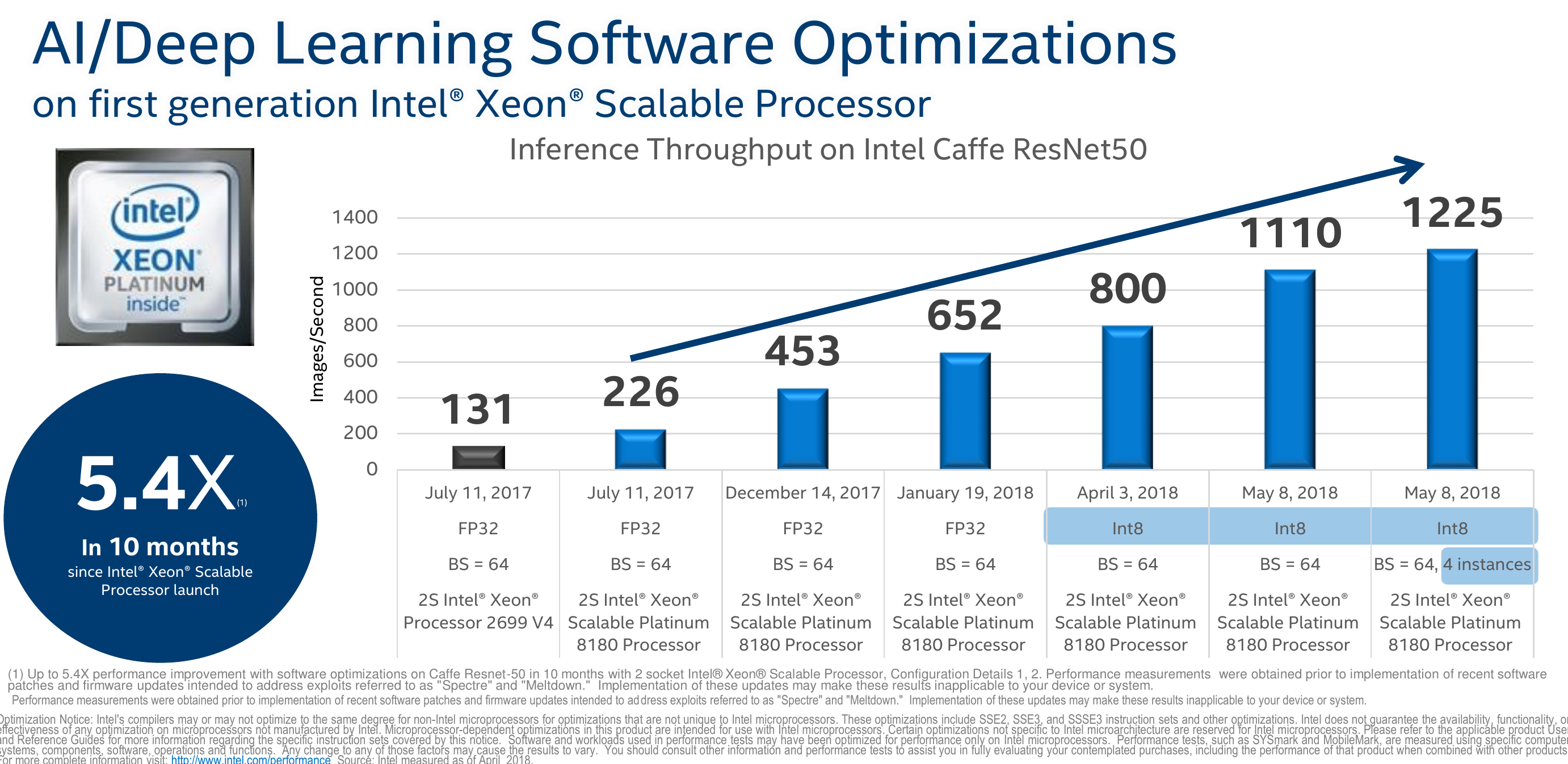
A big component of the performance of the hardware is the software libraries themselves which are often forgotten but must not be overlooked. At Hot Chips, Kumar presented the software optimizations that Intel has been doing with regard to deep learning. Intel claims that since the introduction of Skylake until earlier this year, a 5.4x performance increase was achieved through software optimizations alone. This was done by changing the underlying algorithms, replacing operations with more efficient operations that minimize the memory bandwidth, and by going to an 8-bit integer data type from a 32-bit floating point. It’s a nice reminder that the performance of a machine is a function of all components involved from the hardware itself to the firmware all the way up to the software library.
With Cascade Lake, Intel is introducing a new AVX-512 extension called Vector Neural Network Instructions (AVX512VNNI) which also goes by the marketing name DL Boost. It’s worth noting that in Cooper Lake, DL Boost is extended to also support the brain floating point format.
VNNI introduces two new instructions.
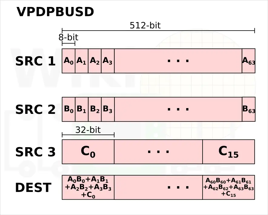
- VPDPBUSD[S] – Multiply bytes (8-bit), add horizontal pair of neighbors
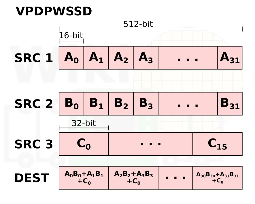
- VPDPWSSD[S] – Multiply words (16-bit), add horizontal pair of neighbors
Both instructions are designed to improve the performance of inner convolutional loops by fusing what is currently two or three individual AVX-512 instructions. Currently, multiplying two pairs of 16-bit values and accumulating the result to 32-bits value requires 2 instructions. This is done by performing an VPMADDWD operation on a set of 16-bit values followed by a VPADD to add the 32-bit result to an accumulate.

Likewise, for 8-bit values, three instructions are needed. 8-bit multiplication is first done using VPMADDUBSW to produce the 32 16-bit values which are then fed through the VPMADDWD and VPADDD operations just as was shown previously. Note that in this scenario, the second source to the VPMADDWD operation is just 1 which effectively converts the values to 32-bit and sums up the neighbors.

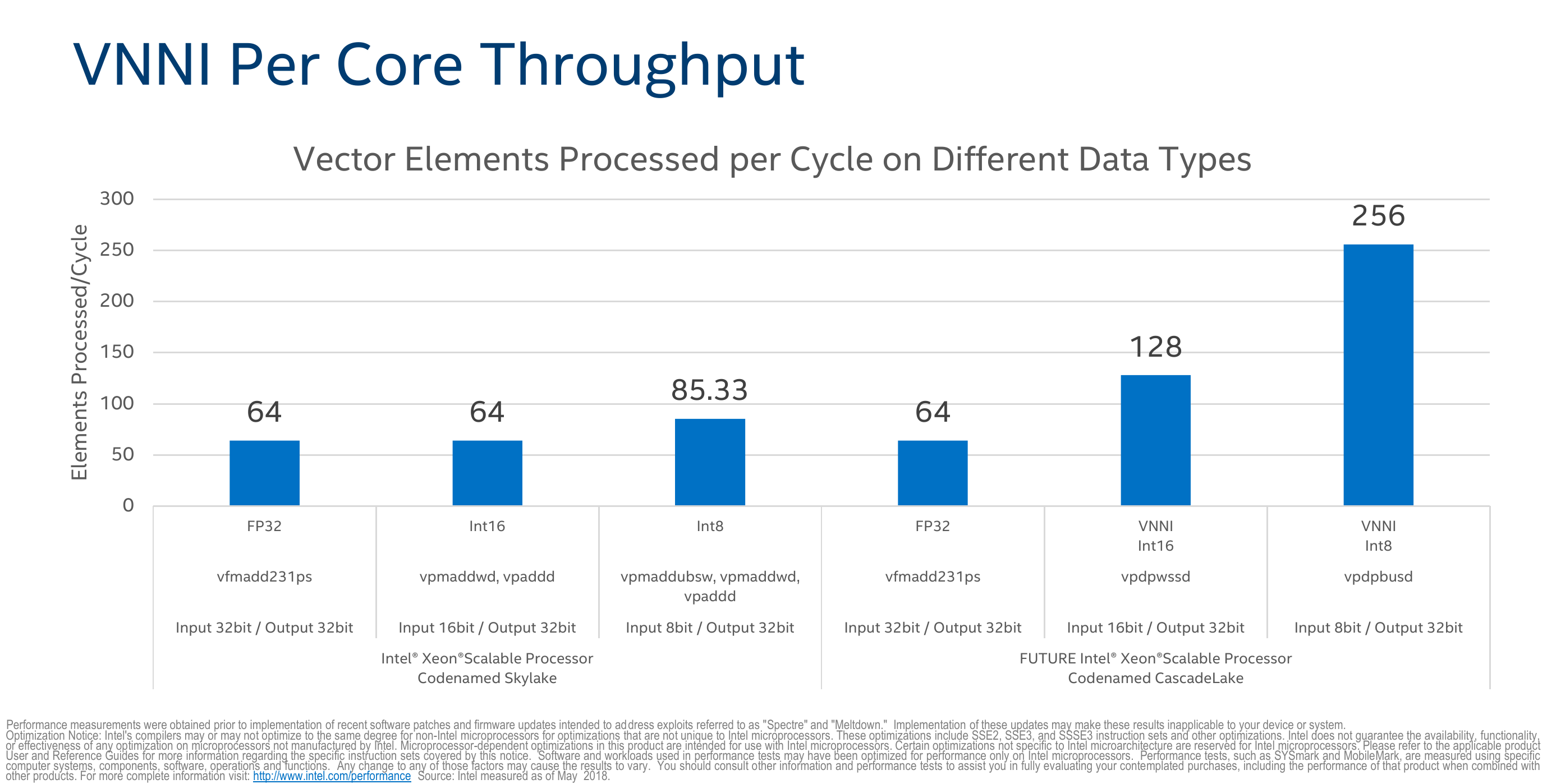
The VPDPWSSD instruction is designed to double the throughput by fusing together VPMADDWD and VPADDD. Likewise, the VPDPBUSD instruction fuses together VPMADDUBSW, VPMADDWD, and VPADDD. One interesting point to make a note of is that both instructions execute in just 1 cycle and can execute on both Port 0 and Port 5 (1|0.5). For comparison, VPMADDWD is 5|0.5.
 |
 |
Cascade Lake AP
Earlier this week Intel made its first disclosure of Cascade Lake AP (Advanced Performance).
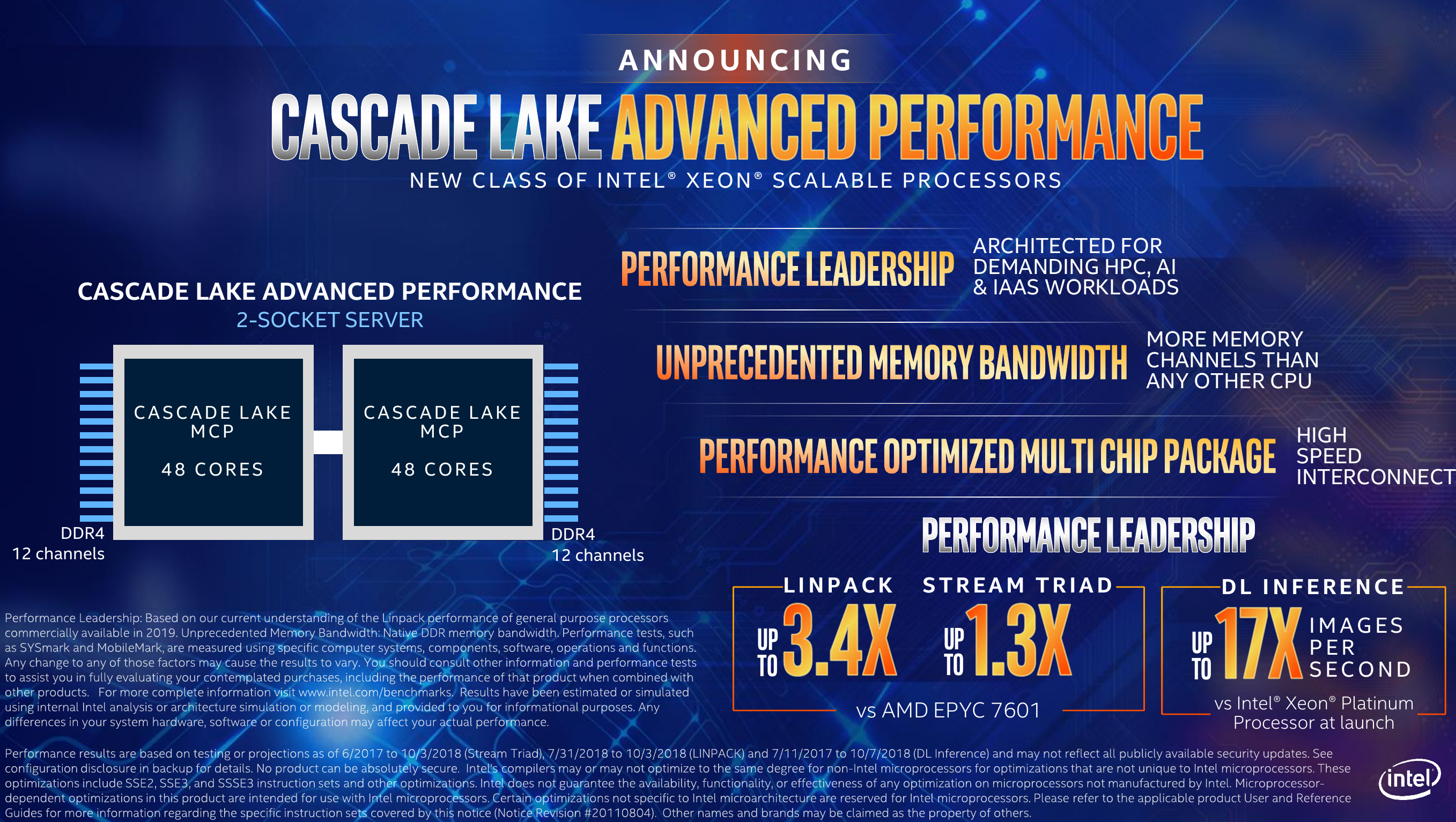
Intel didn’t disclose much about Cascade Lake AP except that it will feature up to 48 cores and 12 DDR4 channels. Though this has not been disclosed, earlier this year Intel’s website did mention that Cascade Lake AP uses a new platform called Walker Pass which uses a 5903-pin flip chip ball grid array (FCBGA) package. Intel has since removed that info from the website though it’s consistent with the leaked roadmap that surfaced earlier this year. Based on that roadmap Walker Pass is set to replace both Knights Landing and Knights Mill Xeon Phis. This suggests Cascade Lake AP actually targets a slightly different market to where Intel’s mainstream Xeons go.
With just two pieces of information – 48 cores and 12 DDR4 channels – we are left to speculate the rest. There are quite a few engineering challenges involved in realizing this kind of chip. The new chip will use two of Intel’s XCC dies, each with up to 24 cores. In theory, Intel can choose to go all the way to 28 cores per die and 56 cores per socket but would require careful power and performance tuning and balancing.
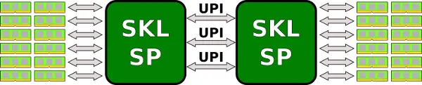
The interconnect between the two dies will make use of Cascade Lake’s existing UPI links. Note there is no EMIB involved. The question becomes what arrangement is being used to link the two dies together. The use of standard Cascade Lake dies on a normal substrate without an EMIB helps reduce design cost and accelerates time-to-market as there is no need to design a new die with a slightly different PHY and bump arrangement. The system costs, unfortunately, will skyrocket with this design due to the power/thermal densities but it might be advantageous for some applications. Currently, Skylake chips support two-way SMP by connecting all three UPI links together.
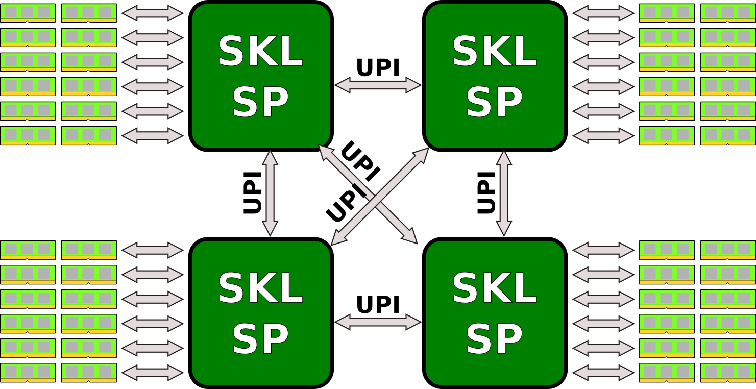
If Cascade Lake AP supports only single-socket configuration then linking the two dies over 3 UPI links in a single package works well. However, if Intel intends on supporting two-way SMP, the way Intel connects four dies together is by connecting one UPI links to every other die. This results in an all-to-all connections yielding very deterministic latency which is something Intel favors.
This suggests that within a single package, one UPI link is used to link the two dies together with four UPI links exposed to the second socket in order to form an all-to-all connection.
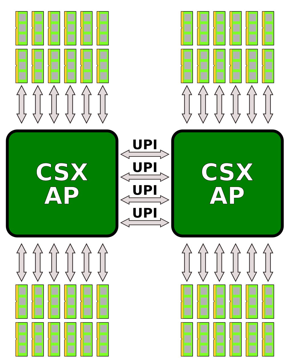
Another mystery concerning Cascade Lake AP is the I/O specs. Each Cascade Lake extreme core count die features 64 PCIe Lanes (4×16). x16 of them are reserved for the on-package Omni-Path Host Fabric Interface (HFI). This leaves 48 lanes exposed for general purpose I/O. With two dies, Cascade Lake AP will likely double this to 96. However, at least in theory, they could reach parity with AMD with 128 lanes if they choose to expose all the available PCIe lanes.
One very strange number we want to point out is the STREAM Triad number. Intel claims Cascade Lake AP is “up to 1.3x” versus AMD EPYC. The problem is, assuming all things equal, this number should be 1.5x theoretical peak performance. The reason for this difference is not clear but it does suggest that only slower data rates are supported or something else is preventing the chip from realizing the full bandwidth of the 12 memory channels.
Cascade Lake AP is already shipping for revenue this quarter to lead customers and will be available for volume shipping in the first half of 2019.
–
Spotted an error? Help us fix it! Simply select the problematic text and press Ctrl+Enter to notify us.
–